Would You Like to Have a Little More? The Power Supply in the Industrial Interface Sector

The EMC challenges an extended IoT system can pose
Figure 1: Schematic diagram of a sensor transmission line in an industrial environment
Summary
This article shows the challenges an extended IoT system can pose in terms of EMC and thus also functionally. Potential leakage currents, inductively and capacitively coupled interference can disrupt data transmissions from wired sensors. To reduce these influences, decoupled, i.e., galvanically isolated interfaces are necessary, which must also be galvanically isolated in the power supply area. The article shows how an additional auxiliary voltage can be generated in a simple way at low cost, which at the same time meets the requirements of galvanic isolation.
Introduction
The wide spread of IoT applications and the decentralization of controls with increased field wiring in industrial use has presented many developers with the challenge of ensuring galvanic isolation, respectively insulation, between the peripheral device, such as a sensor, and the main control. This isolation is critical for signal integrity, system protection and user safety. Thus, galvanic isolation involves isolating both the signal path and the power supply. The topic of this paper will be to show a simple way to provide galvanic isolation of the power supply to sensors, or other peripheral devices.
1. Why galvanic isolation or insulation?
In the industrial sector, widely distributed sensor and control systems are mandatory. Small signal and supply voltages are routed via cables, which are long due to the large spatial separation of the electronics. Communication via wireless connections, such as WiFi, often does not offer a solution, as the high electromagnetic interference potential does not guarantee safe wireless communication. Looking at long cables again, it is found that distortion of signals and interference with the remote power supply often occur in the cables due to various causes, which impair safe operation of the peripherals and sensors to such an extent that safe process control is no longer possible. These causes are:
- leakage currents due to ground loops. They are caused by potential differences between the remote grounded devices (for example sensors) and the likewise grounded control system.
- Coupling of nearby cables, capacitive (du/dt) and/or inductive (di/dt). Power cables that have high load fluctuations, supply large switched inductive loads or feed devices with high interference potential (e.g. frequency converters), coupled interference from the power cable into the signal cable via the parasitic capacitance / negative feedback inductance.
Galvanic isolation of the signal transmission and possibly of the energy supplied via the cable (remote power supply) can prevent leakage currents and significantly reduce the influences caused by interference coupling. However, there are other reasons that may make galvanic isolation necessary:
- The sensor has an electrically isolated structure and must not have any connection to the common ground of the decentralized system in which the sensor operates.
- The sensor must be isolated for safety reasons, to prevent for example high voltages being dissipated.
In order to achieve an effective reduction of interference on the signal transmission as well as on the remote power supply, an impedance-related balancing of the signals and the power supply is necessary. If necessary cable shields have to be galvanically isolated, which means that they have to be connected to the shield ground via overvoltage limiting components. Figure 1 shows an overview of the system.
The measures belonging to Figure 1 are summarized in the following table:
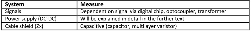
Click image to enlarge
For the purpose of this article, we will limit the focus to the possible measures of the power supply.
2. Different concepts of galvanically isolated power supplies
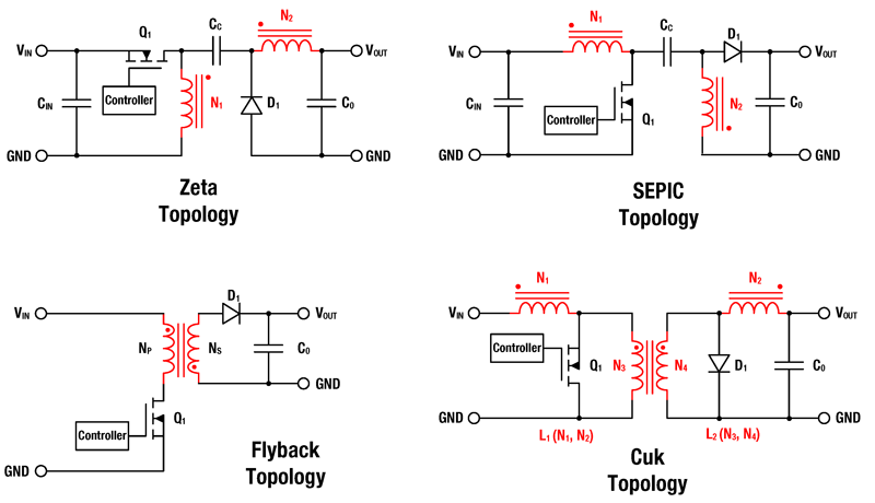
When talking about a power supply with a galvanically isolated output, the flyback converter is referred to in most cases. In general the effort to design a converter is large, especially in the case where "only" an auxiliary voltage is needed for a supply e.g. a sensor. In addition, the circuit design must consider what potential interference is acceptable for this power supply; the circuit design should be chosen accordingly. Figure 2 shows some circuit concepts as an overview.
Click image to enlarge
Figure 2: DC-DC converters of different topologies
Converters in ZETA and SEPIC topology each require a capacitor (CC) as energy storage between the primary and secondary sides of the transformer, so galvanic isolation is only available to a certain limited extent. The Cuk converter allows galvanic isolation, but also requires two chokes for energy storage (N1, N2). This leaves the flyback converter already mentioned as a solution, ..... not the only one! Figure 3 shows another circuit variant which is particularly suitable for the application discussed above, the buck converter with an additional galvanically isolated voltage.

Click image to enlarge
Figure 3: The Buck converter with an additional galvanically isolated voltage
The circuit variant shown in Figure 3 offers the possibility of inexpensively extending a buck converter already present in the circuit design to generate an additional, galvanically isolated voltage. This circuit ("Fly-BuckTM" from Texas Instruments) is an adaptation of the synchronous buck converter topology, where the output inductor (storage choke) is replaced by a coupled inductor, with the coupled secondary output rectified by a dedicated diode and capacitor. In this way, the topology is versatile and offers a range of configurations that can include inverted and any number of isolated secondary outputs. In addition, this circuit option is a cost-effective solution for output powers < 10 W when multiple output voltages that are decoupled from each other are required, as the component cost is very low.
3. Space-saving, low-cost, efficient - the coupled inductor
Coupled inductors are in principle transformers, but differ from them particularly in the fact that they are available with different coupling coefficients. The coupling coefficient, k is a number that expresses the inductive coupling between the windings. It is represented by a number between zero and one, where k = 0 means that there is no coupling and k = 1 means that there is perfect coupling, the following formula shows the relation:
Transformers are designed to transfer energy between windings ideally with minimal losses. However, this requires perfect coupling between the windings without leakage flux, so that the coupling coefficient approaches one. Like transformers, coupled inductors are available in different power classes and with different transformation ratios
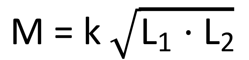
M: mutual inductance
L1: inductance of the primary winding
L2: inductance of the secondary winding
k: coupling coefficient
4. Circuit example, galvanically isolated digital push-pull interface
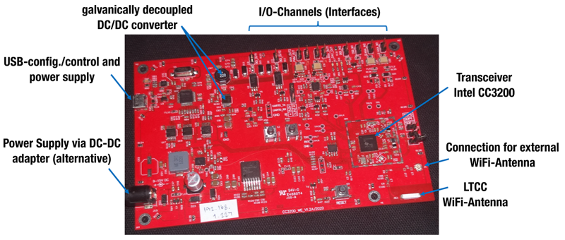
The galvanically isolated digital push-pull interface presented here is part of a WiFi interface board developed as a reference design for various wired interfaces and a WiFi interface. This is used to present applications in the IoT area, Figure 4 shows the board.
Click image to enlarge
Figure 4: Main features of the WiFi interface board
The board can communicate with a second board via a WiFi hub, and the functions of the interfaces can be controlled and monitored through a Windows application. The features are:
- Communication interfaces
- USB 2.0 – interface to the Windows PC
- WiFi – RF interface with Hybrid antenna and alternative connection of an external antenna
- Alternative power supply
- - via USB, or via adapter (9 – 15 VDC)
- Sensor/Actuator - Connections
- 2 analog Inputs, 0 V – 3 V
- 2 analog Outputs, 0 V- 3 V (one optionally configurable as PWM-out)
- 1 DAC- Output via precision Digital to Analog Converter, 0 V – 3,3 / 5 V)
- 1 PWM -> Pulse modulated output, 0 V – 3,3 / 5 V
- 2 Digital inputs, Uin_max: 5 V
- 2 push-pull outputs, galvanically isolated, 5 V / 10 mA
- RGB LED indicator for RF receive signal
- Communication from module to module
- Standalone application for Windows with graphical user interface
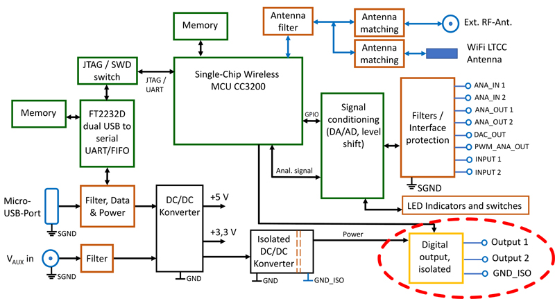
With a compact board like this, the problem is usually that different functional units such as low analog signals, RF signals and digital technology have to be combined in the smallest possible space on the same board. Accordingly, EMC measures are by no means limited to the interfaces. Just as important as interface filtering is the avoidance of coupling between the individual functional units and clean signal integrity of all digital and analog signals. The "interplay" between the signal function blocks, the associated ground system, and the "clean" design determine the amount of work that must ultimately be performed at the interfaces. Figure 5 shows the essential building blocks of the WiFi interface board.
Click image to enlarge
Figure 5: Block diagram of the WiFi interface board, the galvanically isolated interface is marked red
As mentioned at the beginning, in industrial applications there is often the requirement to galvanically isolate interfaces in order to avoid potential shifts or potential leakage currents between devices. An example of a circuit that meets this requirement is realized in this board, in the block diagram in figure 5 the part is marked red, figure 6 shows the circuit diagram.
Click image to enlarge
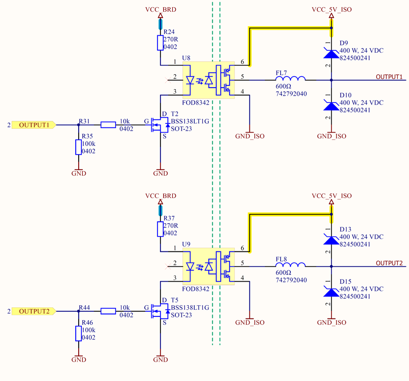
Figure 6: Circuit diagram of the galvanically isolated digital output interface
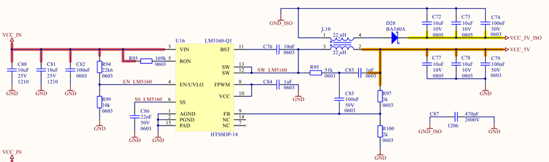
The WE-TVSP Power TVS 824500241 TVS diode is used for overvoltage limitation, and the WE-CBF 742792040 SMD ferrite is used to attenuate the high-frequency interference components. The impedance of the SMD ferrite starts with the resistive range at about 10 MHz and has an impedance of 100 Ω because of the steep rise from about 30 MHz; the total impedance is about 300 Ω at 30 MHz and drops to 200 Ω at 1 GHz. The TVS diodes used to limit high voltage spikes due to transients and inductive loads have a capacitance of 2 x 200 pF, or 400 pF, at a DC bias voltage of 24 V, according to the datasheet. The 400 pF capacitance with the SMD ferrite thus provides a low-pass filter that can effectively filter high-frequency influences from the circuit to the outside, as well as interference coupled into the peripheral cables from outside. The diode clamps at a voltage of 38.9 V and can absorb pulse currents up to 10.3 A. As with all other interfaces wired with surge-limiting components, the TVS diodes must be connected to the reference planes (supply voltage) and ground with low impedance for effective protection. Here, however, the challenge of galvanic isolation arises. To enable isolation, a separate auxiliary voltage must be generated to supply the galvanically isolated push-pull output stages (U8 and U9 in Fig. 6). For this purpose, an output inductor with coupled inductance is used at the DC-DC converter for the +5 V supply "VCC_5V". The circuit diagram of the DC-DC converter with the coupled inductor is shown in Fig. 7.
Click image to enlarge
Figure 7: Circuit diagram of the DC-DC converter with coupled inductance for generating a galvanically isolated auxiliary voltage
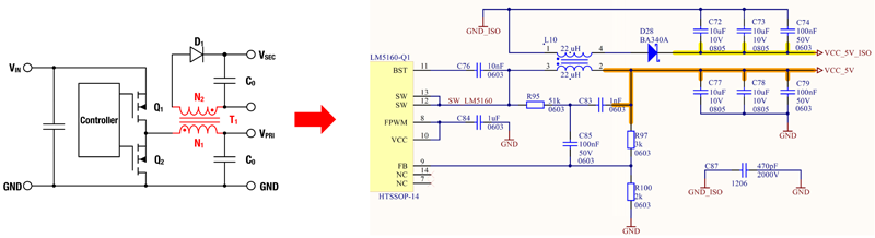
The following is a brief explanation of how the auxiliary voltage is generated with the coupled inductor. The synchronous switching regulator has a synchronously controlled push-pull output stage with a floating high-side gate driver. The low-side FET provides a low-impedance path for the inductor current when the high-side FET is off, thus operating as a synchronous rectifier. Instead of the output inductor typically used, a coupled inductor is now used to provide a second voltage that is galvanically decoupled from the first voltage. The principle is illustrated again in figure 8.
Click image to enlarge
Figure 8: Principle and circuit diagram for generating the galvanically decoupled auxiliary voltage
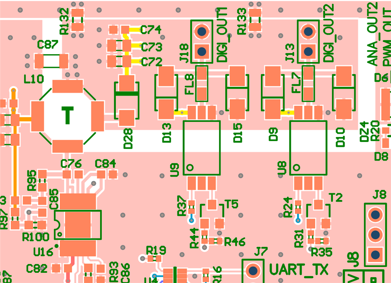
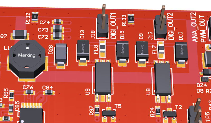
The inductor used here is the WE-TDC HV 8038, No 76889430220 with an inductance of 22 mH per winding and a rated current of 1 A. The inductor is shielded, uses a NiZn based core and has low leakage inductance. The layout and a 3D view of the circuit part are shown in Figure 9.
Click image to enlarge
Click image to enlarge
Figure 9a & 9b: Layout and 3D representation of the circuit section for generating the galvanically decoupled auxiliary voltage
The galvanically decoupled arae is designed as an island through all 4 layers to achieve optimum decoupling. Power supply and digital signals are routed directly on the island and separated via the 3 mm wide trench. The bridging components, R132, R133 and C87 are only for EMC testing of different ground concepts.
5. Conclusion
This article has shown the challenges that an extended IoT system can pose in terms of EMC and thus also functionally. With modern circuit technology, however, even greater challenges in the industrial sector can be solved. For the decoupled, i.e. galvanically isolated interface, the buck converter with an additional winding via a coupled inductance is suitable in the power supply area. In this way, an additional auxiliary voltage can be generated in a simple way at low cost, which at the same time meets the requirements of galvanic isolation. The component portfolio of Würth Elektronik offers a suitable range for this purpose.