onsemi’s Embedded Power Platform (EPP) embeds power die directly into a 12-inch silicon wafer rather than assembling them into a conventional module.
onsemi recently announced what it describes as a breakthrough in power packaging. The company's new Embedded Power Platform (EPP) integrates power die directly into a 12-inch silicon wafer rather than assembling them into a conventional module.
onsemi recently announced what it describes as a breakthrough in power packaging. Allyson Fairchild, EPP Strategic Project Lead at onsemi, said that needs of the industry had driven the innovation, "We're seeing a need for more power in less space, especially in AI data centres, automotive and industrial systems. Designers are being forced into trade-offs between efficiency, heat and cost that become harder to manage as systems shrink.“
The core idea behind EPP is to move the packaging process into the wafer fab. EPP embeds heterogeneous die, which can be silicon, silicon carbide or gallium nitride, directly into a silicon wafer at onsemi's 12-inch fab, then builds interconnect above it. This brings three separate direct electrical benefits.
-
Wafer-level metallisation replaces wire bonds and traditional assembly connections with precise copper layers. The result is substantially reduced parasitic inductance. Fairchild claims that the limitation today is often not the die itself, but getting its performance into the system, adding, "we know what our bare silicon carbide die are capable of, but then packaging it introduces parasitics that degrades that performance".
-
The package is no longer a passive housing. A silicon-based package offers a considerably lower-resistance thermal path than the molded compounds and insulating materials used in conventional assembly. Fairchild highlighted that when using traditional packages, significant areas of the footprint simply cannot extract heat because mold compound sits over the die and spreads no heat at all. With EPP, the entire package conducts, supporting higher continuous power operation.
Additionally, high-voltage isolation is embedded directly into the package using fab-grade processes, reducing reliance on thermally inefficient insulators, negating the need for insulating TIM in data centre applications, or the thick, heavy and expensive DBC substrates beneath automotive power modules. Fairchild claimed that the long-standing trade-off between insulation quality and thermal efficiency can now be resolved in both directions simultaneously.
-
Finally the control circuit can be moved inside the package as drivers and controllers can be embedded alongside power devices, becoming tightly coupled electrically and reducing system-level complexity for the customer.
Another less obvious benefit is quicker development speed. As fab processes are far more precise and repeatable than mechanical assembly, they are easier to simulate accurately. onsemi employs mature digital twin and silicon design simulation tooling to co-optimise electrical, mechanical and thermal behaviour before committing to hardware.
Fairchild explained, "Iterating in hardware is the thing that takes the longest time in the development cycle. Moving that iteration into software should shorten schedules and improve first-time-right rates, which would be a benefit for power packaging.”
The EPP system is very flexible, and technology agnostic. GaN, SiC and silicon die can all be used together in a single chip. Configurations are flexible, with the possibility of multiple die in parallel for lower RDS(on), half-bridge die for EV traction, and power die paired with the controller. External connections allow for tuning, and onsemi can pre-tune designs in applications that make commercial sense. EPP technology has particular relevance for vertical GaN, a technology onsemi is actively developing. To get the very best out of vertical GaN, it must switch as quickly as possible, however, traditional packaging methods with high parasitics make the transistors very difficult to control. Removing a significant amount of parasitics ensures they can perform optimally.
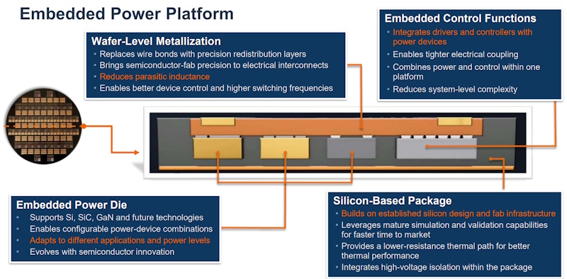
Fairchild expands, “EPP allows us to get more performance out of any die. It enables better device control and higher switching frequencies. The integration of drivers and controllers with the power devices gives really tight electrical coupling. This reduces complexity at the system level, so our customers are getting a product that is easier for them to integrate. We also reduce loop inductance for even better performance.”
Die manufactured on onsemi’s Treo platform can be used to add analog/mixed signal functionality, such as sensor interfaces, control and drivers. In fact, onsemi considers EPP to be the third pillar of the company’s strategy. Power from the die, intelligence from the Treo platform, and EPP integrating the two. Fairchild adds, "we have the power, we have the intelligence, and now we have the integration. EPP enables a true system-in-a-package".
Together, Fairchild estimates that the benefits mentioned above will bring about a 30% board-space reduction in a AI data centre applications through the use of multiple die in parallel, versus a competing solution for the same architecture. The vertical dimension also shrinks, opening up designs that were previously impractical. In automotive applications, EPP should enable smaller, lighter, and more efficient traction inverters, with better thermal performance and lower inductance that will translate into higher range. Beyond those two main applications, onsemi sees fast charging, energy storage, grid modernisation and industrial automation as also benefitting from EPP technology.
Asked directly whether initial yields on such an ambitious programme would need time to mature, Fairchild declined to discuss yield figures but argued the building blocks are established, "we are building this off of existing fab processes. The experience in this fab is already there".
The company also announced Subaru as its first strategic technology partner for the platform, marking the programme's move into the customer evaluation phase. The Subaru engagement gives onsemi technical access to a real automotive programme, with simulation models and engineering samples supplied to support future hybrid and EV architectures.
https://www.onsemi.com/solutions/technology/embedded-power-platform-epp