Gen 3 SiC Devices with Increased Performance and Additional Robustness

A novel trench-bubble design has enabled Bosch Semiconductors' Gen 3 SiC devices to deliver higher performance and greater efficiency while increasing robustness.
Robert Bosch GmbH is the largest Tier 1 supplier in the automotive industry. In addition to manufacturing the subsystems that go into vehicles, the company also makes many of the components it uses in those subsystems. Bosch Semiconductor is a division of Bosch’s Mobility Electronics business sector, which has developed semiconductor technologies, such as MEMS, automotive ICs, and power semiconductors, for over 60 years. Ralf Bornefeld, Senior Vice President and Executive Advisor Semiconductors at Robert Bosch, met with PSD to talk about the details behind the company’s latest Gen 3 SiC devices.
Initially, he talked about the company’s roadmap. It plans on delivering a new generation of products every two years, and has only missed out on that target once, to move Gen 2 from a 150mm to a 200mm process, which Bornefeld describes as taking the same effort as the development of a new generation of products. Gen 3 is scheduled to ramp up early in 2027, with Gen 4 and Gen 5 coming online in 2029 and 2031 respectively.
As for the Gen 3 design itself, Bosch has decided to focus exclusively on trench designs. Bornefeld explains, “We started with trench and we never went planar. Trench technology is better than planar for the individual tuning of devices for performance and robustness. At 3000V and over, the advantages of planar become more competitive, but that is a market that we are not competing in at present. Bosch originally developed trench etching technology in silicon in the mid 1990s. The deep reactive ion etching (DRIE) process is even known as the Bosch process in the industry, and it allows us to etch very steep walls with a high aspect ratio. We then used that 20 years of experience to adapt the deep reactive ion etching technology to silicon carbide, which is a much harder material. That is important, as the more perfect the trench etching is, the easier it is to achieve perfect trench gate oxide making the product robust and reliable.”
Bornefeld explained that the company believes in an evolutionary development of each generation, meaning that it only adds a single major architectural design element to each new generation, building those advances onto each other until it approaches the unipolar limit, which is a material-based limit where it is no longer possible to scale down the on-resistance of the device. Other companies have used superjunction technology for the drift zone, but for now, Bornefeld says the company have enough ideas to approach the unipolar limit without uncorporating it. He adds that the technology is more complex to manufacture, and it changes the switching behavior of the device, as the charge in the drift zone is arranged differently, which requires a different control algorithm and customer training and education. Instead, he believes the company’s evolutionary approach brings a real benefit to customers, as the generational change is not so critical, with the general behavior of the device remaining the same, lowering the risks for customers migrating to the next generation. However, he does add that in Gen 5, the company will incorporate superjunction technology for further gains, but by then, customers will be more familiar with how to handle superjunction devices.
The major design element change in Gen 3 is a p-type shielding region, which Bornefeld refers to as a bubble, implanted at the bottom of the trench before it is filled with gate oxide and isolation material. The bubble provides an increase in performance without compromising robustness. For example, in an inverter application, the short circuit withstand time would be increased, while a planar device with similar performance would have a reduced time.
Other enhancements to Gen 3 devices include a two-zone structure in the JFET region beneath the trench, which acts as a geometrical current constriction between adjacent p-body regions that defines the current path and strongly influences both current density and electric field distribution. Each channel now corresponds to its own JFET region, providing significantly finer control over electric field distribution during both normal operation and fault events. This substantially improves the critical trade-off between on-resistance and short-circuit withstand time (SCWT). The die thickness has also been reduced by 40% to 100 µm, reducing material usage and accelerating heat dissipation. Together, these improvements provide a 20% reduction in specific on-resistance, and around 10% higher short-circuit withstand capability.
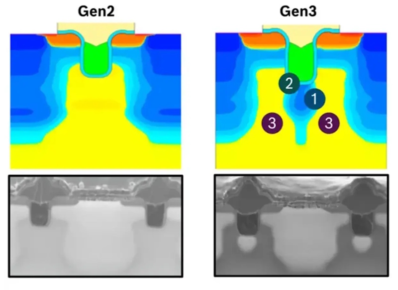
Figure 1 - Advancements in Gen 3 SiC-MOSFET architecture, including the trench (green), the new shield implant below the trench (blue), and the two-zone JFET region (yellow).
Bornefeld concludes by saying, “The change gives the market a lot of confidence in the robustness of our devices, because if somebody buys a product from Bosch, they assume the quality is high, the performance is high, and the robustness is high, and the new element helps achieve this. It will also form the basis of the next generation of devices where it will be combined with another new design element that will further improve the device to approach the unipolar limit. The roadmap is a well thought through sequence of improvements that will get the device to the highest levels of performance, and robustness.”