1250 V/1700 V GaN HEMTs for NVIDIA 800 VDC Architecture

Power Integrations’ PowiGaN technology delivers 1250 V and 1700 V GaN switches, enabling designers to build high-density, high-efficiency power supplies
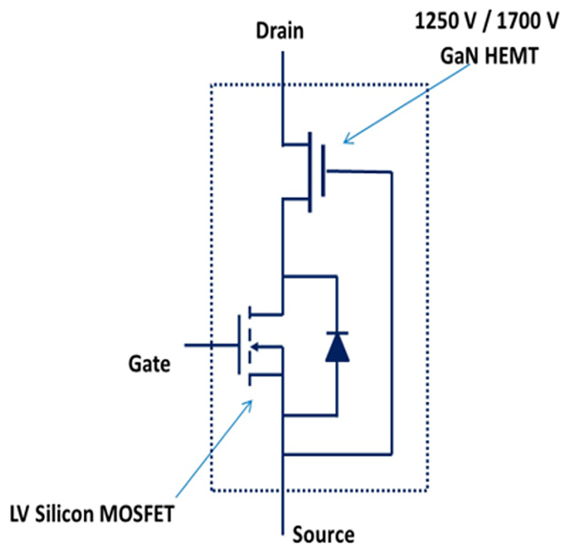
Figure 1: Schematic of a high-voltage PowiGaN cascode switch
GaN-based power semiconductors are ideal for high-efficiency power converters thanks to their superior material properties. However, very few manufacturers offer GaN HEMTs rated above 650 V. The main challenge is that GaN devices built on silicon substrates require very thick buffer layers, which adds significant processing challenges.
As a result, applications demanding wide-bandgap devices at 1200 V and higher have traditionally relied on SiC switches. While SiC meets the voltage requirement, GaN offers a key advantage: much higher switching frequency. This enables the power density needed for next-generation systems—such as AI data centers—while maintaining high efficiency.
GaN HEMTs built by Power Integrations using its proprietary PowiGaN technology are uniquely capable of overcoming these limitations. They achieve up to 1700 V voltage rating in a practical device, making them a compelling alternative to 1200 V SiC and beyond.
With a 1250 V PowiGaN cascode switch, power supply designers can specify an operating peak VDS of 1000 V, while allowing for industry-standard 80% de-rating. For applications up to 1360 V, the 1700 V PowiGaN device is available.
1250 V / 1700 V GaN HEMT Cascode Switch
The 1250 V / 1700 V GaN HEMTs are normally-on, depletion-mode devices. To achieve the normally-off operation required for safe system design, each GaN HEMT is connected in series with a low-voltage silicon MOSFET in a cascode configuration (see Figure 1). This approach eliminates the need for a p-type GaN gate layer, avoiding threshold voltage drift and related instability issues—ensuring long-term reliability.
Click image to enlarge
Figure 2: Typical off-state characteristics of the 1250 V and 1700 V PowiGaN cascode switches
Off-state characteristics for typical 1250 V and 1700 V PowiGaN cascode switches are shown in Figure 2, demonstrating stable leakage behavior well beyond their rated voltage. This provides excellent transient overvoltage capability and a significant safety margin compared to similarly rated silicon or SiC devices.
Ensuring Field Reliability
Extensive reliability evaluations—covering both static and dynamic conditions—have been performed on the 1250 V PowiGaN GaN HEMT:
High Temperature Reverse Bias (HTRB)
This off-state stress test assesses long-term stability under high drain-to-source bias and accelerates thermally activated failure mechanisms under strong electric fields over an extended period. Tests performed in accordance with JEDEC JEP198 HTRB specifications on the PowiGaN HEMT show excellent device leakage stability.
Additionally, intrinsic off-state failure rates were modelled under accelerated VDS conditions. Results predict a cumulative failure rate of 1 ppm in >15 thousand years of operation at 1000 V / 100 °C, demonstrating a substantial reliability margin.
High-Voltage High-Humidity High-Temperature Reverse Bias (HV-H3TRB)
For high-reliability deployments, a controlled high humidity environment is used as an additional stress factor. The HV-H3TRB test examines failure modes in passivation layers, active regions, termination design, and underlying structures. Again, when tested in accordance with JEDEC standard JESD22-A101, the 1250 PowiGaN switch maintained identical leakage stability as observed during HTRB.
Dynamic High-Temperature Operating Life (DHTOL)
Dynamic RDS(ON)stability during high-voltage switching is critical for GaN devices. Poorly designed GaN HEMTs often exhibit significantRDS(ON) increase during high-voltage switching transitions due to electron trapping, reducing efficiency and risking hard failures.
The RDS(ON) of the PowiGaN 1250 V GaN cascode, monitored for 1000 hours of DHTOL stress at 1000 V/125 °C, showed stable performance comparable to state-of-the-art 650 V GaN HEMTs. This demonstrates that PowiGaN HEMTs can be scaled to well beyond 1200 V without compromising performance—including the critical hard-switching capability— making it robust for high-reliability applications.
NVIDIA 800 VDC AI Data Center Architecture
It is becoming increasingly clear that high-voltage DC (HVDC) distribution will replace the conventional 54 V DC bus architecture in AI data centers. A proposal from the Open Compute Project (OCP)—initiated by Google, Meta, and Microsoft—defines an 800 VDC power system. This new architecture transforms power delivery, scaling from the traditional sub-100 kW per rack to 1 MW per rack.
Industry leaders are already moving in this direction. NVIDIA, for example, has publicly discussed and evaluated 800 VDC architectures for next-generation AI data centers. By adopting a direct 800 VDC input, compute racks do not need conventional integrated AC-DC PSU stages. Instead, racks accept two-conductor 800 VDC feeds and use high-voltage isolated DC-DC converters within the rack to supply xPU subsystems. This approach removes rack-level AC-DC conversion blocks, simplifying rack design while boosting performance.
The combination of simplified topology, fast switching speed, and robust voltage capability makes 1250 V and 1700 V PowiGaN technology an excellent fit for these new architectures.
1250 V and 1700 V PowiGaN technology’s combination of simplified topology, fast switching speed, and robust voltage capability makes it ideal for these new applications. The following sections compare the value propositions of 1250 V and 1700 V PowiGaN devices—first against stacked 650 V e-mode GaN solutions, and then against 1200 V SiC MOSFETs.
1250 V PowiGaN vs. 650 V e-mode GaN
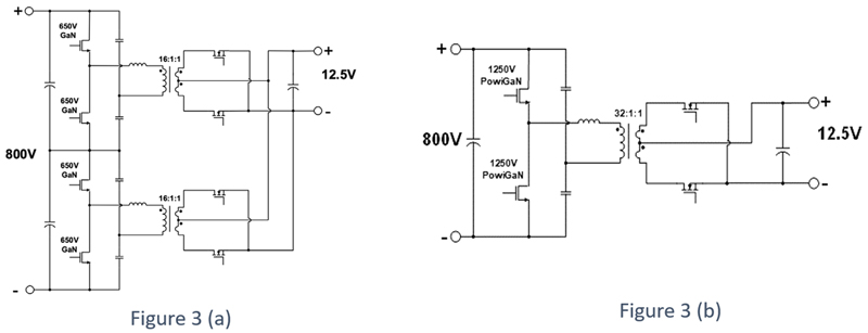
Figure 3 compares an 800 VDC input to 12.5 V output fixed-ratio LLC topology using 650 V e-mode GaN versus 1250 V PowiGaN. Both solutions leverage fast-switching GaN devices to operate at frequencies above 500 kHz with an 800 VDC input. However, for 650 V e-mode GaN, a stacked LLC converter is required to handle the 800 VDC input.
On the primary side, this architecture uses two stacked half-bridges in series, requiring four 650 V e-mode GaN switches. On the secondary side, outputs are paralleled so each half-bridge supports half the total output power. This stacked topology introduces several challenges:
• Input voltage imbalance:Input voltage imbalance during normal operation must be carefully managed. If it occurs between the half-bridges, the stress voltage across the GaN devices can exceed the expected ~400 V. This causes more pronounced dynamic RDS(ON) degradation due to current trapping effects within the HEMT’s 2DEG channel.
• Complex drive design: Each half-bridge needs a dedicated high-side driver and isolated bias supply, increasing cost, space, and design complexity.
• Less efficient and higher cost:With identical RDS(ON) devices, the stacked topology suffers higher conduction losses than a single half-bridge using 1250 V PowiGaN. In fact, PowiGaN can use lower-cost HEMTs with 2× higher RDS(ON) while still achieving the same efficiency profile.
Click image to enlarge
Figures 3: (a) 650 V e-mode GaN-based stacked half bridge LLC; (b) 1250 V PowiGaN-based single half bridge LLC
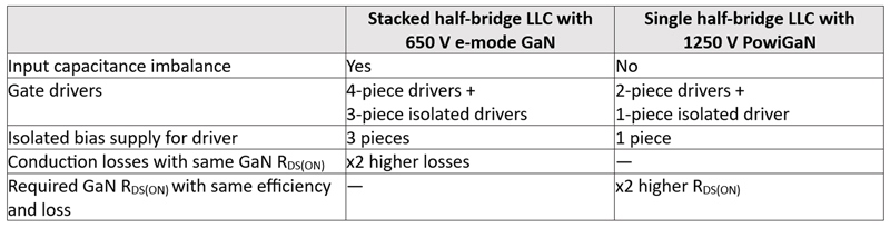
Differences between 650 V e-mode GaN and 1250 V PowiGaN in a half-bridge LLC application are summarized in Table 1.
Click image to enlarge
Table 1: Half bridge LLC comparison between 650 V e-mode GaN and 1250 V PowiGaN IC
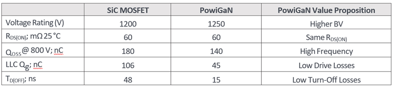
1250 V PowiGaN vs. 1200 V SiC MOSFET for 1 MHz LLC Operation
To achieve high power density, operating the LLC converter at high frequency is essential. Maximum operating frequency depends on several key parameters:
• QOSS (Output charge)
• Qg (Total gate charge)
• TD(OFF) (Turn-off delay time)
Lower values for these parameters directly improve efficiency and power density in LLC designs.
Table 2 compares 1250 V PowiGaN with 1200 V SiC MOSFETs. The conclusion is clear: 1250 V PowiGaN enables significantly higher operating frequency for LLC converters compared to 1200 V SiC MOSFET devices with similar RDS(ON).
Click image to enlarge
Table 2: Parameter comparison between 1200 V SiC MOS and 1250 V PowiGaN
1700 V PowiGaN for HVDC AI Data Center
In 2024, Power Integrations introduced the industry’s first 1700 V PowiGaN-based product, designed to support 1000 VDC nominal input voltage while meeting auxiliary power requirements for HVDC AI data center architectures. The IMX2353F (520 mΩ at 25 °C) device from the InnoMux™2-EP product family (Figure 4) incorporates both primary- and secondary-side controllers, protection and sense elements, and a safety-rated feedback mechanism (FluxLink) into a single IC that features a 1700 V PowiGaN switch. By independently regulating and protecting up to three outputs, it eliminates multiple downstream conversion stages.
The IMX2353F device operates exclusively in DCM SR-ZVS mode, featuring zero-voltage switching (ZVS) on the primary switch. This significantly reduces parasitic capacitive discharge losses during turn-on, improving thermal performance—a critical advantage for 800 VDC to 1000 VDC input ranges.
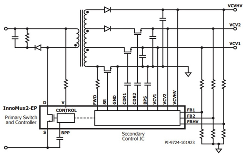
Click image to enlarge
Figure 4: Typical application of IMX2353F
With 1700 V PowiGaN and SR-ZVS control, temperature rise is limited to only 22.3 °C at 1000 V input and full power, enabling a compact, cool-running auxiliary power supply for HVDC AI data centers. This device is particularly well-suited for the increasingly popular 48 V fan implementations in 800 VDC PSUs, where 12 V system outputs are also required.


