Solving the thermal challenge for new designs no longer needs to be a significant challenge
Power engineers often face seemingly conflicting and almost impossible challenges. As system designers add more features and functionality to newer product generations, so the system requires more power, but has less space available to generate it. While there are many techniques available to manage heat, forced air cooling is often unreliable and draws in dust that can lead to premature failure. Passive cooling using heatsinks meanwhile is reliable, but requires space and adds weight that is often just not acceptable in modern equipment that is designed to be portable. As such, solving the thermal challenge is often a significant challenge on new designs.
The best approach to thermal management is not dealing with the waste heat, it is to find more efficient approaches so that the heat is not generated in the first instance. Correct selection of the topology and, more importantly, the power switching components, is critical to achieving this. However, all power circuits generate some heat, no matter how efficient they are.
As designs get smaller, the opportunities for passive convection cooling are reduced and designers have to find innovative ways to thermally connect semiconductor junctions heat spreading surfaces and ultimately to the ambient environment where the heat can dissipate.
However, the impact of package selection is not limited to thermal performance - packages with longer leads introduce parasitic elements into the circuit that can affect both the speed of operation and efficiency.
A novel approach to cooling small packages
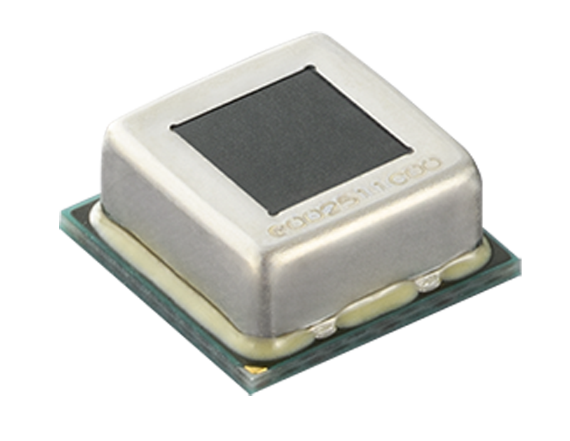
ON Semiconductor is one company that has developed a power-specific packaging technology to address the need for improved thermal performance in today’s electronic designs. ‘Dual Cool’ technology is based on Power Quad Flat No-Lead (PQFN) packaging and creates a direct heat path from the drain and source sides of the vertical MOSFET die structure. This structure facilitates adding a heatsink alongside direct thermal conduction into the printed circuit board (PCB).
Dual Cool has evolved from the popular and established PQFN packaging. While implementing new features, the Power33 and Power56 lead geometries and pinouts are retained, allowing designers to improve thermal performance without having to change the PCB layout, thereby facilitating an easy transition.
By replacing wire bonds with copper clips that are similar to leadframes, Dual Cool improves the thermal conductivity and current handling of the package. As a result, higher power densities are possible.
A standard PQFN package with clip technology offers a 13.9% improvement over a traditional wire bond-based PQFN package. Adding Dual Cool technology increases the performance differential to 57.5%.
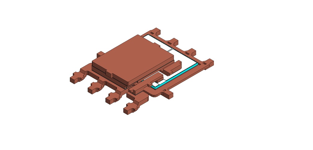
Dual Cool uses four mils thin silicon, which is half the normal MOSFET thickness, thereby improving thermal and electrical performance. The top and bottom surfaces of the die are plated to permit solder attachment of the drain lead frame on the bottom, and the source and gate clips on the top. To improve the heat transfer path from the die to the top of the package, a heat slug is soldered to the source clip. Solder attachment of the silicon to the lead frames, with optimized copper clips additionally reduces electrical and thermal parasitics.
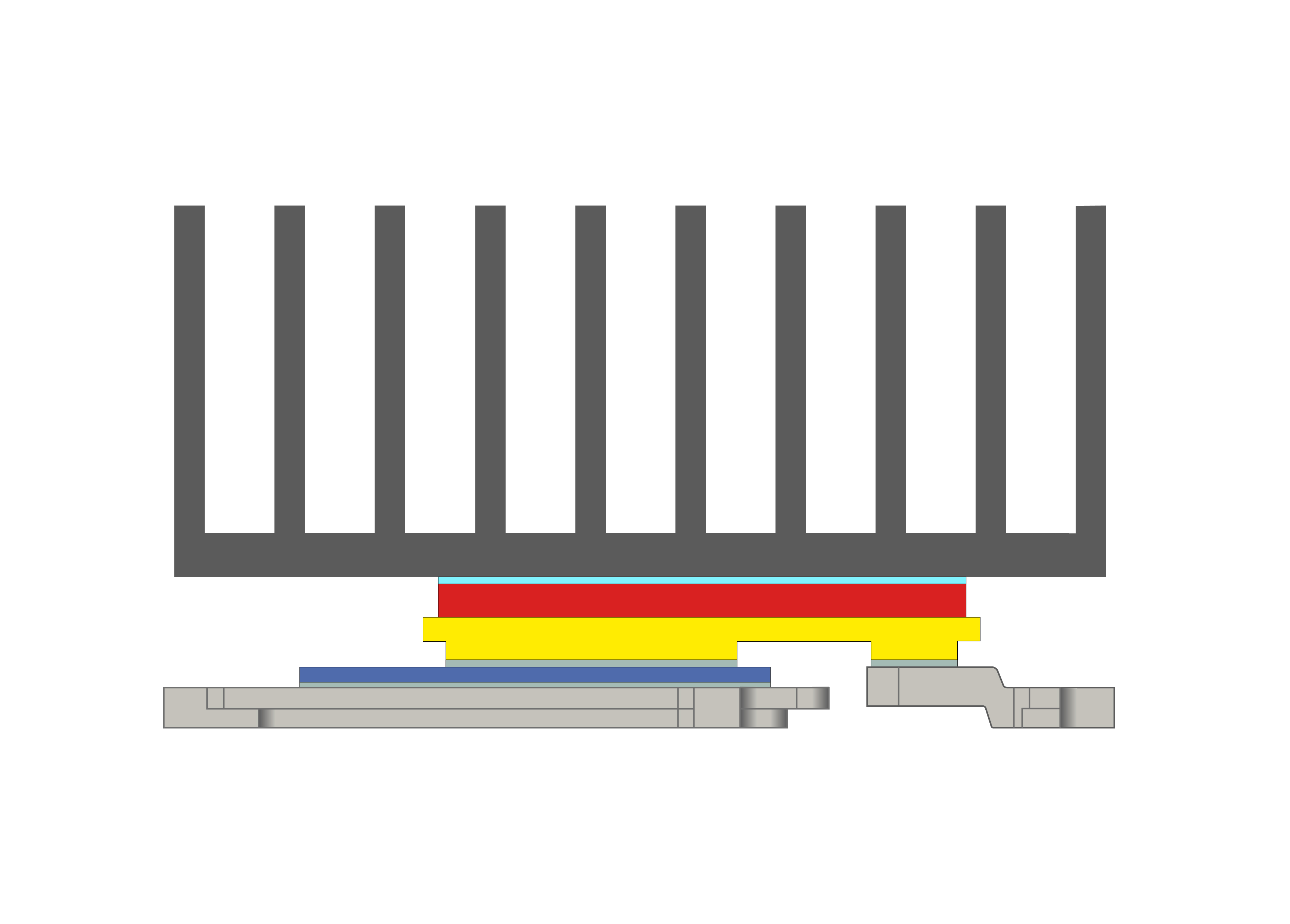
Click image to enlarge
Figure 2: Dual Cool is ideal for use with a heatsink
The θJC (thermal resistance from the junction to the case) has two important aspects: the junction to case thermal resistance to the drain tab as well as the top heat slug. The datasheet contains these values for each specific product type, giving a measure of the two most efficient heat paths out of the component, allowing the designer various options for managing the thermal energy created by high power density designs.
Dual Cool and PowerTrench MOSFETs
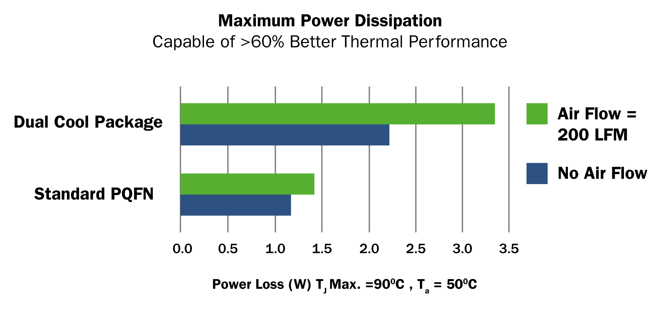
ON Semiconductor's PowerTrench MOSFETs offer excellent electrical properties including very low levels of RDS(on) making them a good choice to benefit from the new Dual Cool packaging concept. The integrated monolithic SyncFET Schottky body diode is ideal for power applications. The combination of Dual Cool and PowerTrench occupies the same land pattern as PQFN-JEDEC standard parts, yet allows for >60% better thermal performance as shown in Figure 3.
Click image to enlarge
Figure 3: Users can achieve a 60% performance improvement
Dual Cool PowerTrench MOSFETs with top-side cooling have a far better thermal coupling to the top of the device. In many cases, they can be used without an additional heatsink thereby reducing size, cost and weight. With enhanced dual-path thermal performance and improved parasitics over its wire-bonded predecessors, the use of a heatsink provides even more impressive results.
Laboratory testing has shown that when a heatsink is used with Dual Cool package technology, synchronous buck converters deliver higher output current and increased power density. With ON Semiconductor's trench silicon technology, Dual Cool packaging gives excellent results in terms of both power density and thermal performance.
Click image to enlarge
Figure 4: Dual cool technology embedded in a PQFN package
The Dual Cool product portfolio from ON Semiconductor offers more than 20 products with BVDSS values from 25 V to 150V and multiple choices for RDS(on) and package size. All Dual Cool solutions are lead-free, RoHS-compliant, and available in 3.3 mm x 3.3 mm, 5 mm x 6 mm, and 8 mm x 8 mm PQFN packages.
Dual Cool and Heatsinks
Heatsinks are a very effective method of further improving thermal performance, especially if there is airflow across their surfaces.
Many styles and shapes of heatsinks are available and selection of the appropriate solution will depend on the application, available space and heat to be dissipated. Attachment methods include solder anchoring, push pin, thermal tape, screwing, or glue / adhesive – the selected method will depend on the products selected end use criteria, and any available processes at the manufacturing site.
Thermal interface materials (TIM) such as those listed below can be used to improve the contact between the Dual Cool package and the heatsink and eliminate any possibility of air gaps in the interface that will limit heat dissipation.
● Thermal Grease
● Insulating Pad
● Phase-change Materials
● Thermal Tape
● Gap Filler Sheet or Gel
● Thermally Conductive Glue or Adhesives
Testing and evaluation by On Semiconductor demonstrated that thermal grease provides an improvement over gap filler sheets primarily due to the thin interface. Wire bonded packages showed a 10% improvement over gap pad, which rose to 12% for clip bonded packages. For Dual Cool, performance was shown to be improved by 21% over the Gap Pad.
The result is that a device that can dissipate 5.8 W with a thermal Gap Pad, can dissipate 7.0 W with grease, with no other changes. However, grease may be the best performance-wise, but is more difficult to dispense, rework and does not have the electrical isolation properties of the pad. The application will dictate if these trade-offs are worth making.
In applications where tightening a screw, a push pin, or a solder anchor is used to secure the heatsink, a compression load is placed on the component. The PQFN 8 x 8 Dual Cool package has been tested and simulated to withstand high compression loads. Results show that the package can withstand up to 1500 N of load without causing any electrical or mechanical failure.
Board layout and production
Due to their small size and low profile, PQFN packages are an ideal space-saving alternative to leaded options. Additionally, the Dual Cool PQFN offers a size advantage over the industry standard D2PAK SMD package.
Looking in more detail, the source and gate pads are larger than the package lead to allow toe filleting of the solder. The pads are also wider than the leads, to account for variation in board fabrication and component placement during assembly. Combined, these tolerances can stack up to 0.10 mm.
The PCB pad for the exposed thermal pads is the same as the size of the exposed pad allowing the surface tension of the molten solder to pull the component so that it perfectly aligns with the land pad. This process ensures that the Dual Cool packages are consistently and correctly aligned during production.
In power applications where significant heat is generated, the PCB pads act as a local heatsink, transferring thermal energy into the board itself.
When performing thermal characterization of PQFN 8 x 8 Dual Cool packages, it was demonstrated that there is a significant improvement in the thermal resistance from junction to ambient if the copper on the PCB is increased to a larger (say 1in2) copper pad connected to the solder-mask-defined land pad. This approach is recommended for the drain pad.
Summary
By combining innovative Dual Cool packaging with high performance PowerTrench technology, engineers are now able to access products that firstly minimize heat generation by operating very efficiently and, secondly, have the ability to move any excess heat to the edge of the package.
In fact, in many applications, due to the efficient performance the Dual Cool / PowerTrench, devices can be used without additional heatsinking reducing size, weight and cost of the system solution.
On Semiconductor