Are you SiC of Silicon? - Part 1

Part 1 of a 6 part series: Application Trends in SiC
Anup Bhalla, Ph.D., Vice President Engineering, UnitedSiC
SiC applications began in the 2000s with the adoption of SiC JBS diodes into PFC applications. This was followed by the use of SiC diodes and FETs in the PV industry. But the recent surge in applications relating to EV On-board chargers and DC-DC converters is driving SiC growth. The nascent adoption in the EV inverter, 650V devices, and adoption in server supplies and 5G telecom rectifiers promises rapid growth. This article examines the advantages of these SiC devices over incumbent Si technologies.
SiC Device Benefits
Advantages of using SiC FETs over IGBTs have been amply demonstrated. The wider bandgap of 4H-SiC allows formation of voltage blocking layers with ideally 100 times less resistance than corresponding unipolar silicon devices. SiC also has 3X the thermal conductivity of silicon. SiC MOSFETs with steadily improving performance are now available from 650-1700V, both as planar and trench structures, but still suffer from poor MOS channel mobility. SiC JFET based cascode FETs are also available, with smaller chip sizes resulting from the higher bulk mobility of the SiC JFET channel.In the remainder of this article, we refer to all these SiC transistors as SiC FETs, unless there is a need to differentiate between the two, since they can be used interchangeably in most instances.
At 1200V and above, silicon MOSFETs give way to IGBTs, which provide a lower conduction loss at high load currents, but since the lower conduction loss results from conductivity modulation, this comes with a penalty in switching losses. IGBTs are typically used with anti-parallel fast recovery P-i-N diodes, which also contribute to switching losses, since the stored charge in these diodes must be removed before the diodes can sustain an off-state voltage. Figure 1a compares the on-state characteristic of a UnitedSiC FET compared to a typical 200A, 1200V IGBT. At all operating conditions below 200A, lower conduction losses are possible with SiC, especially given the absence of a knee voltage. Figure 1b compares the third quadrant characteristics in freewheeling mode for IGBTs with Si FRDs, UnitedSiC FETs and SiC MOSFETs. In the absence of an anti-parallel or integrated SiC Schottky diode, the conduction loss for SiC MOSFETs is much higher than for FRDs typically used with IGBTs. Both the SiC MOSFET and Cascode FET offer low QRR operation (often 10X lower than Si FRDs). Therefore, SiC FETs can switch much faster than their IGBT counterparts, but synchronous switching is a must for SiC MOSFETs to avoid excessive 3rd quadrant conduction losses.
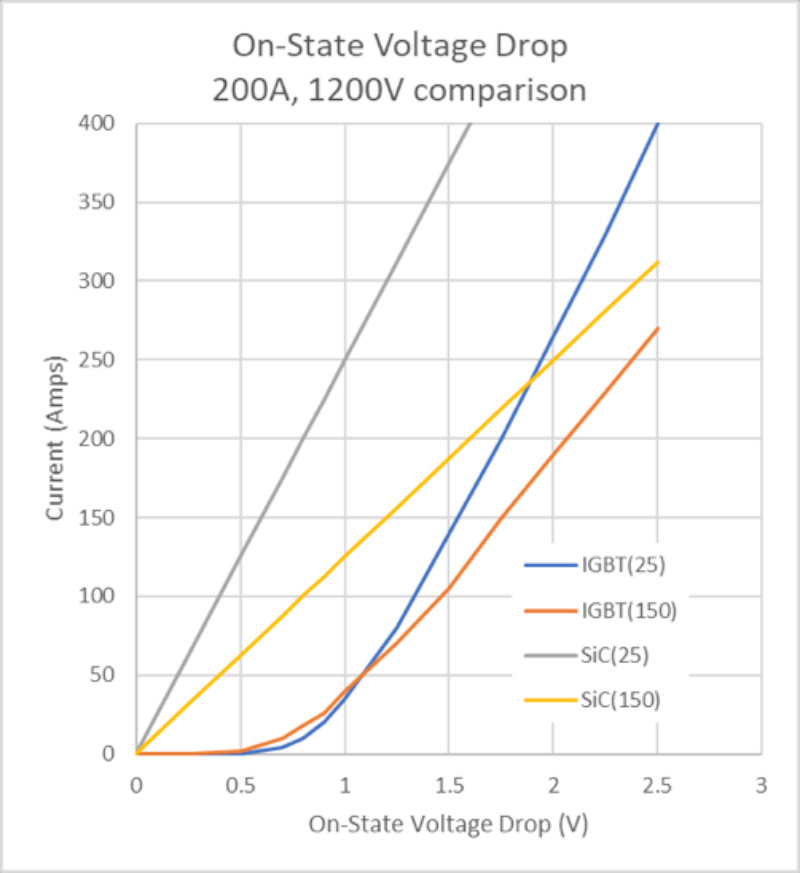
Click image to enlarge
Figure 1a: On-state voltage drop of SiC FETs vs IGBTs in first quadrant conduction
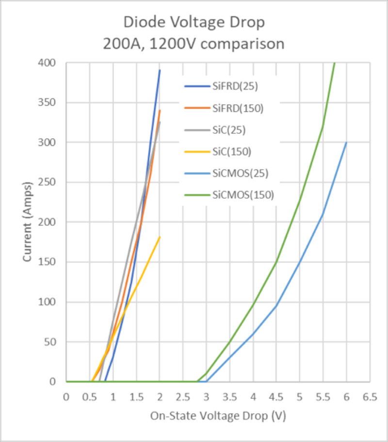
Click image to enlarge
Figure 1b: Typical 3rd quadrat conduction characteristics of Si FRDs used with IGBT, UnitedSiC FETs and typical SiC MOSFETs without the use of anti-parallel Schottky diodes
SiC Diodes in PFC and Boost converters
The use of SiC diodes in PFC circuits and boost converters is widespread, because the absence of stored charge leads to much reduced EON losses in the FET, whether that is a 650V superjunction MOSFET at 400V bus voltages, or a fast IGBT at 600-1500V bus voltages. In fact, the advantage of using a SiC JBS diode increases with voltage. Even without the use of SiC FETs as the main switching device, these diodes offer a path to increased efficiency and higher operating frequency, which explains the >$100M market for these well-established products.
SiC advantages in hard switched circuits
Table 1 captures the key datasheet parameters of interest when evaluating switch technologies for hard switched applications. Let’s take a few important cases. For server power supplies, telecom rectifiers and on-board chargers that operate with bus voltages of 400V, the totem-pole PFC topology, or 3-phase active frontend rectifier may be used depending on power levels. To improve power density and cut BOM costs, higher switching frequencies are needed to reduce inductor size. High EON losses preclude the use of silicon superjunction FETs in continuous conduction mode (CCM), even those with lifetime reduction applied to reduce QRR, due to excessive losses and poor recovery characteristics. All the SiC FET solutions offer excellent low QRR diodes, and consequently, much reduced EON losses. Used with Kelvin source packages like TO247-4L, D2PAK-7L and DFN8x8, designers can push for 2-3X higher hard switching frequencies than obtained with Silicon. It also helps that all SiC FET options have a lower TCR, i.e. a smaller increase of on-resistance with temperature.
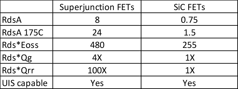
Click image to enlarge
Table 1: Key parameters useful for assessing technologies for hard switching
SiC Benefits in soft-switched circuits
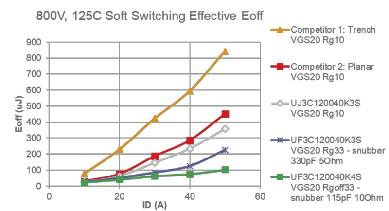
The use of the phase-shift full-bridge and LLC circuit for DC-DC conversion is widespread, both in server power supplies and telecom rectifiers, as well as EV on-board chargers and DC-DC converters. The value of wide-bandgap switches in general, and SiC based FETs in particular in these applications come from a few main characteristics. First, SiC FETs have low Coss, which allows a fast VDS transition at turn-on, which then allows the use of high switching frequency or wide input/output voltage ranges. Second, the turn-off loss with soft turn-on switching may be estimated as the measured hard switched turn-off energy minus the energy stored in the output capacitance, expressed as EOFF-EOSS. and as shown in figure 2, the turn-off energy is extremely low for SiC FETs like the UF3C120040K4S. Third, low RDS(ON) values combined with high voltage ratings enable operation of DC-DC converters at 800V. Fourth, SiC FETs have low reverse recovery charge and very high voltage slew rate capability, in the range of 100 to 200 V/ns. This practically eliminates dv/dt induced failures without resorting to carrier lifetime reduction. Finally, UnitedSiC FETs in particular have a low body diode voltage drop, typically only 1.5 V, compared with 3 to 5 V for SiC MOSFETs and GaN HEMTs. As the frequency rises, the percentage of time the body diode conducts increases, making the conduction loss of the diode during the dead time more significant.

Click image to enlarge
Figure 2: Effective turn-off loss (EOFF – EOSS) for various SiC FET options. A loss of 100µJ at 50A, 800V means that the device only generates 10W of turn-off switching loss at 100kHz when used in a PFSB at that current. At lower currents, these low losses allow frequencies up to 500kHz
SiC Benefits for EV Traction Inverters
All the loss benefits of SiC FETs in hard switching can benefit EV traction inverters, but if the operating frequencies for the motor drive are low, the main benefit must come from lower conduction losses. This was already shown in Figures 1a and 1b, stemming from the low resistance per unit chip area, and unlike IGBTs, a lack of a knee voltage in forward conduction along with the possibility of synchronous reverse conduction.
A key characteristic of the switch needed for EV applications is to withstand short circuit faults of various types. This requires the switch to withstand the entire bus voltage (400V for 650V devices, 800V for 1200V devices), while simultaneously conducting a high current when the gate is fully on, for a period of 2-6µs until the de-saturation circuitry detects the short condition after an applied blanking time of 0.5 to 2µs. Then the driver tries to softly turn the switch off. During this time, the switch may experience a temperature rise of 300-500 °C in a few µs, and must turn-off safely nonetheless. Furthermore, the switch should handle up to 100 or 1000 such events with no shift in device parameters.
While this characteristic is offered for IGBTs, SiC MOSFETs and GaN HEMTs struggle to meet the same levels of robustness. UnitedSiC cascode FETs are unique in their ability to safely handle repetitive short circuits with minimal tradeoff in chip size or on-resistance. This stems from the intrinsic characteristics of the normally-on JFET, which, being a bulk conduction device, has no gate oxide to degrade, and can withstand higher temperature and electric field peaks than SiC MOSFETs. Furthermore, the decrease in channel conductance from self-heating rapidly reduces the device current, slowing the rate of heating and allowing the device to last longer before failure.
SiC devices are generally more robust in this mode, since these vertical devices absorb the heat in their volume, whereas GaN HEMTs are lateral devices that develop the heat in the ultra-thin 2-D electron gas.
SiC Benefits in linear mode applications
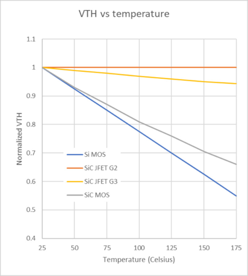
Figure 3 shows the normalized VTH vs temperature characteristics of SiC normally-on JFETs, SiC MOSFETs and Si MOSFETs. It is clear that only the normally-on SiC FET avoids VTH decreasing with temperature. If a device is being used as a current source, or even in a solid-state breaker where it is deliberately switched slowly, time spent in the regime of low current, low |VGS-VTH| and high VDS can cause devices with negative VTH temperature coefficients to be susceptible to current filamentation, and failure at much lower voltages than expected. This is not the case with SiC JFETs, and this fact has been experimentally verified. Therefore, SiC JFETs become very useful to form current sources, electronic loads etc., where they must be biased in this low current high voltage dissipation regime without destruction all the way to its rated breakdown voltage.
Click image to enlarge
Figure 3: Effective turn-off loss (EOFF – EOSS) for various SiC FET options. A loss of 100µJ at 50A, 800V means that the device only generates 10W of turn-off switching loss at 100kHz when used in a PFSB at that current. At lower currents, these low losses allow frequencies up to 500kHz
SiC Benefits for circuit protection
The fact that VTH does not decrease with temperature, the excellent current limiting and short circuit capability of SiC JFETs, and the ability of SiC JFET devices to withstand 4X higher energy dissipation than silicon devices before destruction, makes these devices very useful in circuit breakers, inrush current limiters and as load switches. JFETs offer the lowest available RDS(ON) at a given chip size with lower operating conduction losses, without compromising the robustness of these devices to withstand repetitive overstress events.
A novel approach to flexible high voltage FETs
UnitedSiC has demonstrated the supercascode approach to high voltage FETs, where very high voltage switches have been built by series connecting many normally on-JFETs with a low voltage Si MOSFET and a unique bias network, that yields a composite device that can be used as a 3-terminal switch. Recent developments targeting a 200A, 6500V Half-bridge module have been constructed with 5 stages of 1700V JFETs in series. The device may be switched with a single 0 to 12V gate drive with low Qg – there is no need for separate gate drives as with series connected IGBTs or SiC MOSFETs. Another demonstration, for a low current switch, applied the supercascode technique to a 40kV single switch. Since the lower voltage JFET technology is more mature, and the starting material less costly, this offers designers the option of lower cost solutions up to voltages previously unattainable. Alternatively, if a particular voltage or current class is needed and not available, it can be constructed readily with UnitedSiC cascode and JFET devices.
Click image to enlarge
Figure 4: Normalized change in VTH with temperature for Si MOSFETs, SiC JFETs and Si MOSFETs. A negative slope leads to unstable operation for low |VGS-VTH| at high VDS. This problem does not exist for SiC normally-on JFETs
Conclusions
We have tried to cover a lot of ground in this article, explaining briefly the benefits seen with SiC FETs and SiC JFET based solutions for a wide range of applications. More information on these subjects can be found on the UnitedSiC website and publications. Not only can SiC FETs improve your design for high frequency DC-DC and AC-DC applications, but UnitedSiC FETs offer drop-in capability into your existing silicon based designs, due to the wide operating gate drive range. The benefits of UnitedSiC FETs in EV inverters, from low conduction losses to robust short circuit handling were explained. Active mode and circuit protection applications, especially for high voltage and power are a unique niche for SiC JFET technology, as well as building flexible high voltage high current switches using lower voltage JFET building blocks. Future articles will provide more insight into these application areas – please stay tuned.