Are you SiC of Silicon? – Part 4

Part 4 of a 6 part series
How to Build Better EV Traction Inverters with SiC
In this article, we examine the benefits of applying SiC technology to EV traction inverters. We show how the efficiency of the inverter is boosted under all loading conditions, from light to full load. Using higher operating voltages with efficient 1200V SiC FETs can help cut copper losses. It is also possible to increase inverter switching frequency to output more ideal sinusoidal waveforms to the motor windings and reduce iron losses in the motor. All these factors are estimated to enhance the range of the BEV by 5-10%, while simplifying the cooling problem by cutting losses
Introduction
Recent news makes it clear that the uptake of battery electric vehicles (BEVs), is faster than previously estimated. This has prompted renewed effort by automobile manufacturers, both incumbents and start-ups, to examine the best technologies to extend range by maximizing efficiency, reducing size and weight, and extracting the maximum benefit from the expensive battery pack. This has led to rapid penetration of SiC transistors into the on-board charger and DC-DC converters in EVs. Given that the traction inverter processes 10X that level of power, if SiC transistors offer a similar benefit in that space, it will transform the power semiconductor landscape. For that to happen, SiC technology has to provide a clear cost-performance benefit, and clear all the requisite hurdles to allow for a reliable and manufacturable inverter system design. The boost stage used before the inverter will no doubt use SiC, for the same reasons as we’ve previously discussed for on-board chargers and DC-DC converters. In this article, we examine the key benefits of SiC technology for the EV inverter and discuss several implementation schemes based on UnitedSiC technology.
Key Benefits of SiC Technology
The drive cycles of a typical EV, especially those used in urban environments, cause the inverter to be used in the light to mid-load range for most of its operating life, but with frequent stops and starts. Yet the inverter must be designed for all the worst-case stresses such as rapid acceleration, climbing steep inclines, and operation across a wide range of ambient temperature conditions. Figure 1 shows a typical two-level voltage source inverter that might be used to drive an internal permanent magnet motor. This is a commonly used configuration for BEVs, with the inverter placed close to the motor. Typically, the inverter switches are controlled such that a 3-phase AC voltage is applied to the motor windings. This is done by turning the power switches on and off as commanded by the controller, at frequencies of 4-10kHz, to produce a fundamental AC frequency up to 1kHz. Total power levels may range from 50-250kW for passenger EVs. The DC voltage used depends upon the battery system, and since a boost converter is used to convert the variable battery voltage to a fixed DC voltage for the inverter, this voltage may go from 300-500V today, to 600-800V in the near future, with higher voltage allowing delivery of the same power with lower current and reduced copper losses.
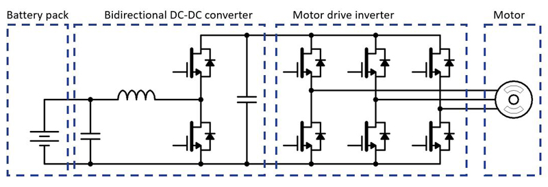
Click image to enlarge
Figure 1: EV traction inverter using a 2-level voltage source converter architecture
The losses in the power switches therefore come in the form of conduction losses that occur while the switch carries current, as well as switching losses, that occur when the switches turn-on and off. Conduction losses do not depend on switching frequency, but switching losses are directly proportional to the frequency used.
Figure 2 shows the characteristics of SiC FETs versus silicon IGBTs. At any given current, the conduction loss is given by the ID*VDS product. It is therefore easy to see that with the unipolar SiC FETs, the absence of a knee voltage seen with IGBTs is beneficial at all current levels up to 200A, but especially beneficial at lower currents corresponding to light and medium load operation.
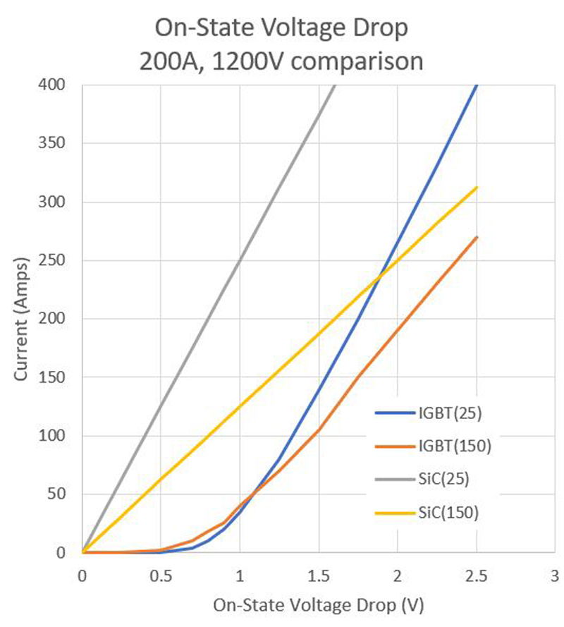
Click image to enlarge
Figure 2: Conduction loss characteristics of 200A SiC FETs and IGBTs
Figure 3 is a chart comparing the conduction and switching losses of a low conduction loss IGBT and SiC FET based inverter for 750V devices operating from a 400V bus at 8kHz. The IGBT solution has considerable switching losses even at 8kHz and can therefore not be used efficiently at 25kHz. The SiC based solution not only offers lower conduction losses at all output levels, with much reduced losses at 8kHz, but can also be used at higher inverter frequencies with better efficiency.
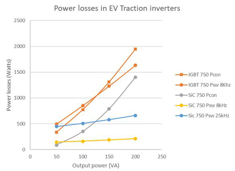
Click image to enlarge
Figure 3: Comparison of power losses, conduction and switching, for inverters based on 1200V IGBTs and SiC FETs. The difference in losses is seen under all conditions, but is quite large at 25kHz
Another aspect of EV inverters, that differs from traditional industrial motor drives, is the need for bidirectional power transfer. During regenerative braking, the switches are controlled to allow the same inverter to act as a rectifier, while the motor acts as a generator, thereby allowing power to flow back to the battery. The fact that SiC FETs allow third quadrant conduction with the same low conduction losses means that synchronous rectification can be employed to keep losses very low in this mode of operation as well. This is not possible with IGBTs, and anti-parallel freewheeling diodes handle the reverse power flow with higher losses.
Voltage ratings
A significant number of EV inverters today are based on 750V IGBTs to operate inverters with bus voltages in the 300-500V range. To more efficiently process high power, 1200V switches would allow the use of 600-800V battery voltages.
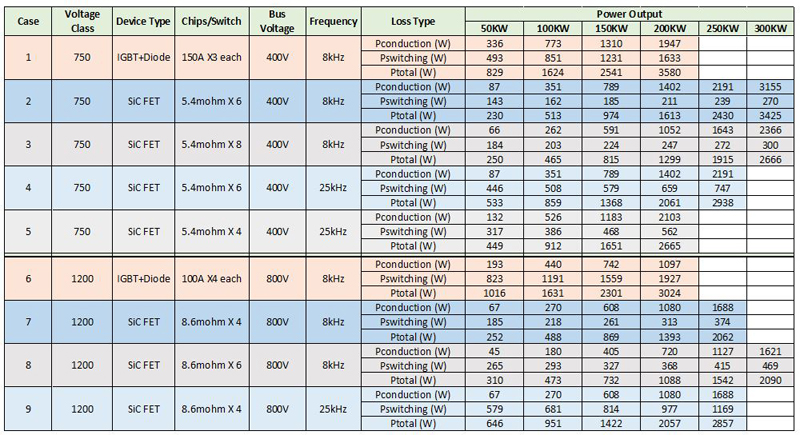
Table 1 examines some calculations for a 450A, 750V half-bridge module used in a 200KW BEV traction drive based on low conduction loss IGBTs, and UnitedSiC FETs also rated at 750V. Each switch position uses 3 IGBTs and 3 Diodes. These are replaced with 6 Stacked SiC FETs, each 5.4mohm in resistance but less than half the size. Case 1 and 2 show the difference in total conduction, switching and total losses at 8kHz. The totals losses are halved at 200kW, while they are nearly a quarter at 50KW. Given that the inverter operates in light load most of the time, this is quite beneficial. Note that both the conduction and switching losses are lower with SiC FETs, but the difference in switching losses is nearly 8X at 200KW. It is also shown that the same module can be used for up to 300KW keeping all FETs below Tj=150C, which allows the use of the same inverter hardware for a 300KW system. Case 3 shows an even better way to handle 300KW with 8x SiC FETs per switch, cutting peak losses from 3425 to 2666W.
Click image to enlarge
Table 1: A comparison of operating power losses of a 450A, 750V 3-phase inverter module used in a 200kW EV inverter, based on 750V IGBTs versus one based on 750V SiC FETs. The bottom half compares the 400A, 1200V IGBT module with a corresponding 1200V SiC FET module used in a 200kW inverter. In all cases, we pin fin heatsink type 3-phase module is considered with coolant temperature of 90C. Maximum junction temperature is kept below 150C in all cases, even though SiC FETs are rated for 175C and can handle 200C short duration usage.The lower switching losses can be used to run the inverter at 25kHz, improving waveform quality and reducing motor iron losses. Even in this condition, the SiC FET solution can be seen (case 4 Table 1) to have lower losses than the IGBT solution across all load conditions. At 200KW output, the IGBT solution dissipates 3580W at 8kHz, while the SiC FET solution dissipates 2061W at 25kHz. The module allows 250KW output within 6x paralleled SiC FETs
It is possible to trade of losses for lower cost by using just 4X SiC FETs per switch. This is shown in case 5 of Table 1, and losses remain well below that of the IGBT based solution.
The lower portion of the table compares losses if 1200V transistors were used and the operating bus voltage was 800V. 4 IGBTs and 4 Diodes per switch (Case 6), compared to 4X SiC FETs per switch (Cases 7,9). Losses at 8kHz with the SiC FETs are less than half at full power, and 4x lower at 50KW output. Case 8 shows how with 6X SiC FETs per switch, the same module can be extended easily to 300KW operation. While it would be impossible to switch these IGBTs at 25kHz due to excessive switching losses, case 9 shows how this can be accomplished with SiC FETs, while maintaining high efficiency. Losses remain well below that of IGBTs operating at 8kHz, and again, the smoother waveforms can help drive down motor iron losses, while the inverter switches well over audible range. In all instances, note that the module offers higher power output in the same footprint.
Extreme conditions
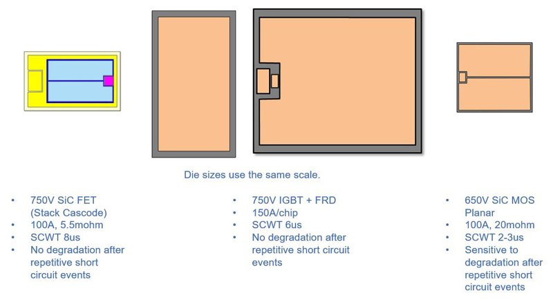
An important safety requirement of all motor drives, including EV inverters, is the ability to withstand a short-circuit that could occur during maintenance or operation. Such shorts may occur across the DC bus, across a motor winding to ground, or between windings. For the semiconductor switches, this means that the switch may have to survive turning on into a short circuit until the gate drive detects the condition and turns off the switch within 3-5µs. Alternatively, a short circuit might occur while the switch is already conducting. In any case, the switch must be able to withstand these events, no matter the chip starting temperature when this event occurs, with no change to device characteristics that degrade its lifetime.
Figure 4 compares the difference in short-circuit withstand time (SCWT) of IGBTs, SiC MOSFETs and SiC FETs. SiC MOSFETs suffer from extremely high peak currents in short-circuit, which can damage the MOSFET gate oxide. This can be managed by using a lower gate voltage drive, which reduces short circuit currents, but at the expense of considerably higher conduction loss. The SiC FET, which consists of a Si MOSFET stacked on a SiC JFET, does much better in this regard. With minimal change in conduction loss, the peak saturation current can be adjusted to provide the needed short circuit withstand time. This saturation current is set by the JFET and is therefore independent of the VGS applied to the MOSFET. Experiments have shown that this type of stress can be safely handled by the SiC FET for over 100 repetitive events. In addition, devices will handle such short circuits even when the starting chip temperature is 200°C.
Click image to enlarge
Figure 4: A comparison of short circuit capability of IGBTs, SiC MOSFETs and SiC FETs, as well as a ranking of ability to handle repetitive strikes
The semiconductors in figure 4 are drawn to scale, with the SiC FET being the smallest chip size 100A device. The ability to withstand the intense heat generated during the short circuit is a key benefit of SiC JFETs, which for the base of the SiC FET stack cascode. The chip size difference also explains why one can reduce on-resistance so much in a given module footprint using SiC FETs.
Technical Approaches to SiC based inverters
The most popular topology of the inverter is the venerable 2-level voltage source converter of figure 1. The type of switching used with such an inverter is called hard-switching, and results in considerable overlap of high voltage across and current through the switch during transitions. One approach designers can take, based on the results of figure 3, is to use the fast switching SiC devices to reduce both switching and conduction loss, even at frequencies up to 25kHz. In that case, the switch transitions occur at high dV/dts. In BEVs, there is no problem with long cable lengths between inverter and motors as in standard industrial drives. However, high dV/dt waveforms directly applied to motor windings may cause large displacement current in the insulation. This can be rectified using a filter at the inverter output, to smooth just the high dV/dt parts, as with a so-called dV/dt filter, or a complete sinus filter, that smooths the waveforms to provide a near perfect sinusoidal output. Clearly, filtering is easier if the switching frequency is higher. Reducing the ripple in the current waveform is projected to provide an improvement in overall motor efficiency by a 1-3% and extend motor life. This efficiency benefit can be translated into extended range or reduced battery sizes.
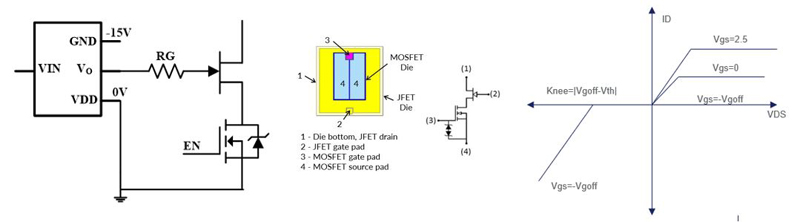
Another approach could be to maintain switching at low frequencies of 5-8kHz and operate the device at very slow dV/dt rates, for e.g. below 8V/ns. In that case, switching overlap losses per cycle can be high, but the low frequency keeps total power loss manageable. Figure 5 shows the preferred technique to use SiC FETs in this situation. The stacked low voltage MOSFET is simply used as an enable switch to ensure normally-off operation under start-up and short-circuit fault conditions, but the SiC JFET gate is switched on and off directly. That allows very low dV/dts to be achieved with optimal losses. This scheme allows for excellent short circuit handling capability, and it can reduce conduction losses further by 15-20% if the JFET gate is driven to +2.5V instead of 0V. For managing third quadrant conduction, either the JFET can be used with low dead times, or small JBS diode can be added to carry freewheeling current during the dead time only. The graph on the right of Figure 5 shows the third quadrant behavior of the SiC JFET.
Click image to enlarge
Figure 5: A switching scheme for directly driving the JFET gates and using the stacked N-channel MOSFET as an enable switch. This allows easier implementation of low dV/dt switching
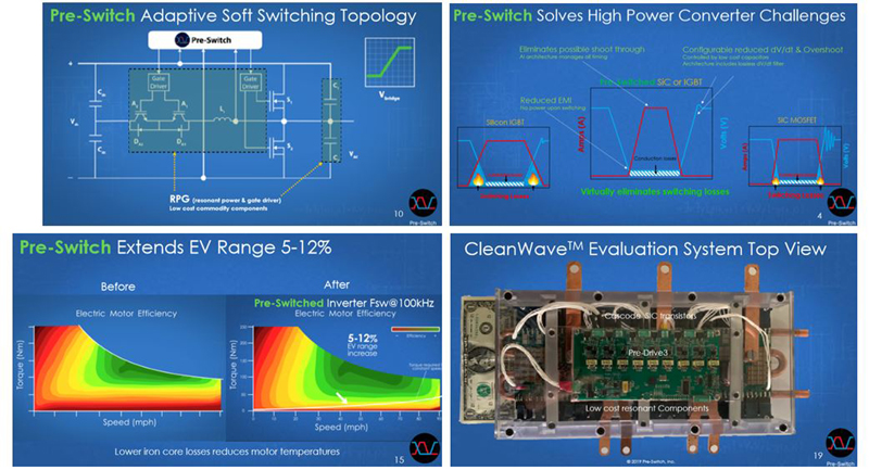
A more complex approach, but one which can achieve the highest efficiency, is to apply full resonant switching as with the auxiliary-resonant commutated pole method, for which a novel controller has been developed by Pre-Switch Inc. Figure 6 shows circuit topology and typical switching waveform, which results in the complete elimination of turn-on and turn-off switching losses while maintaining low dV/dts. While this circuit can help reduce IGBT switching losses and improve efficiency, IGBTs still suffer from losses caused by the need to remove the stored charge in each cycle. Furthermore, the conduction loss impact of the knee voltage in the IV curve remains. Therefore, peak efficiency across all load conditions is still best achieved by SiC FETs, which are unipolar devices with no tail current and no knee voltage. The converter can also be operated at very high frequencies 50-100kHz, resulting in much smoother output sinusoidal waveforms. This could further boost motor efficiency by cutting iron losses, which combined with the minimal power losses of the inverter provides the maximum range extension for the BEV. An example of a compact 200kW inverter using this method with SiC FETs can be seen in figure 6.
Click image to enlarge
Figure 6: The ARCP topology to eliminate all switching losses in inverters. This allows very high-power densities to be achieved with SiC FETs, without the problems of high dV/dt switching. The result is improved motor operating efficiency as well as high inverter efficiency
Conclusion
In depth investigations by many industrial and academic groups have concluded that SiC MOSFETs offer a clear advantage for improving the efficiency of traction inverters and extending the range of BEVs. We discussed the reasons for this assessment in this article, and considered the robustness needs of the power transistors used in SiC inverters. We looked at three implementation topologies for the BEV inverter, which allow users to select the method that fits their overall system constraints best. For the highest efficiency, the ARCP scheme eliminates all switching losses, and allows the maximum use of the ultra-low conduction losses offered by SiC FETs.
UnitedSiC