Part 5 of a 6 part series
Ultra-High Voltage SiC and Supercascodes
New applications are emerging that require high voltage switch technology which is significantly lower in balance-of-system costs and operating losses than silicon IGBT and IGCT technology. This spans a wide range from solid state transformers, MW motor drives, to smart grid applications (FACTS, STATCOM) and HV DC-breakers. SiC MOSFETs are considered excellent choices to disrupt this space in the near future and UnitedSiC offers a unique approach to accelerate the adoption of WBG-based high voltage switches. This approach is called the Supercascode. We compare this approach, and its demonstrated performance, to what can be achieved with silicon technology and silicon carbide MOSFET technology.
SiC Devices and Modules
In the last decade, many advances have been made in high voltage SiC devices. In theory, SiC devices can be developed to reach at least 10X the maximum voltage ratings of silicon devices. Along these lines, many demonstrations have shown single SiC MOSFETs up to 15KV, and even SiC IGBTs up to 27KV. MOSFETs in the 6.5KV-10KV range are now emerging as module-based products. It has been amply demonstrated that SiC MOSFETs offer dramatic loss reductions relative to silicon IGBTs above 3.3KV.
For 10-25KV voltage SiC IGBTs, challenges of carrier lifetime enhancement and control, growth of ultra-thick epitaxial layers, device reliability and optimal characteristics are being researched, with products still 5-10 years in the future.
In >3.3KV space, the main device structures currently used and being developed are the planar MOSFET and the MOSFET with integrated Merged P-i-N Schottky (MPS) diode shown in figure 1. The latter device removes the need for additional SiC Schottky diodes in the module, enabling more space for packing in MOSFETs and increasing the available current ratings, since the increase in chip size to add the Schottky region within each cell is modest. However, due to the high current ratings needed for the target applications, relatively large devices with active areas of 0.5-1cm2 are needed, which are hard to make at high production yields in SiC.
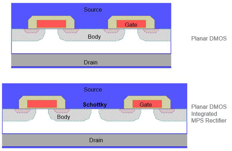
Click image to enlarge
Figure 1: Structure of the Planar MOSFET (a) and MOSFET with integrated Schottky (b) being developed for higher voltage SiC applications. Many such devices need to be paralleled in a module to achieve the desired current rating, and each chip switches the full bus voltage
One key challenge with high voltage devices is that thicker epitaxial layers result in a greater number of defects in the starting epitaxial wafers. These thicker and more lightly doped layers have wider doping variations, since it becomes more difficult to maintain tight doping control as doping levels reach 1014cm-3 levels. With increasing thickness, there is also a higher cost of consumables during epitaxy. The current state of the art has achieved high quality for 30um epitaxial layers up to 3.3KV devices, and 6.5-10KV (50-90um) layers are being enhanced to reach production quality in the next few years. Epitaxial layers for ratings of 1.7KV and below are available with very high quality and tight parameter distributions on 6inch 4H-SiC substrates.
Many interesting challenges emerge when packaging ultra-high voltage switches. When a single switch operates from a 5KV bus, and switches off in 25ns, we get a dV/dt of 200V/ns. A 10pF stray capacitance (for e.g. from the chip drain to the baseplate, or across the gate circuit isolation barrier), would cause a 2A (C*dV/dt) displacement current per chip. Since high powered modules tend to have many (10-20) chips in parallel, this problem can become quite severe. These stray currents cause additional losses and can also cause serious mis-triggering problems with the low voltage gate drive electronics. Excessive displacement current flow can also weaken insulation both within modules and in the external cabling and circuitry.
In 10KV rated devices, the 10KV is dropped across a 1mm zone atop the device termination. This requires very careful attention to the device encapsulation and cleanliness during module manufacturing to avoid air pockets, partial discharge, as well as any disruptive electrical potentials in the vicinity of this field from bus bars and bond wires. Thick ceramics are also needed to isolate the switches from the baseplate, and this results in increased thermal resistance. For e.g., using a single ceramic DBC for 15KV devices would require well over 1mm of AlN thickness. Field distribution of traces on the ceramic must be well managed to control partial discharge and eventual catastrophic shorting from the chips in the module to the baseplate.
Supercascode? What and Why.
UnitedSiC has developed a unique approach to making high voltage SiC devices using a Supercascode concept based on series connection of multiple lower voltage devices, operated with a single gate driver. Let’s examine the fundamental logic behind this approach. Table 1 shows the resistance of 1cm2 SiC JFETs vs. breakdown voltage rating. Consider the example of trying to build a 6500V, 12.5mohm module using 6500V devices in parallel. That would require 4 chips with 1cm2 area each connected in parallel. Alternatively, we could achieve the same resistance by placing 4 of the 1cm2 3mohm, 1700V chips in series (3x4 = 12mohm). So, the series solution essentially uses the same amount of SiC, but the lower voltage devices are obviously lower in cost and easier to manufacture with higher yields and better parameter distributions.

Click image to enlarge
Table 1: Specific on-resistance of SiC JFETs from 1700V to 30KV. Note that 4x series connected 1cm2 chips would have the same resistance as 4 paralleled 6.5KV chips. This is the basic logic of the Supercascode approach
While the same concept can be used with SiC MOSFETs, each low voltage module would need its own synchronized gate drive. This adds complexity. With the Supercascode method, a single low voltage MOSFET at the bottom of the series chain controls the entire series switch. In so doing, the gate charge requirements of the Supercascode method become a lot lower than the need to drive paralleled HV MOSFETs or even series connected HV MOSFET modules. Table 2 compares the characteristics expected from Supercascode modules to equivalent modules made by paralleling SiC MOSFETs.

Click image to enlarge
Table 2: Comparison of a Supercascode module to one made by paralleling SiC MOSFETs with integrated Schottky diodes. Note the differences in gate charge
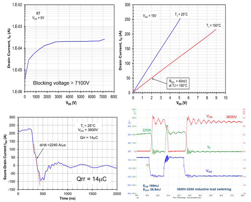
While many implementations have been devised for the Supercascode, figure 2 shows two circuits that have been developed by UnitedSiC. The module requires a passive balance network, which is embedded within the module as shown in Figure 3. Since the dissipation is dominated by the SiC JFETs, they are placed on the DBC for efficient heat removal. The other network components are in the PCB layer, above this layer. Figure 4 shows the electrical characteristics of this Supercascode module being developed at UnitedSiC. The devices block the required voltage, on-resistance is 20mohm (25 deg C), and no SiC JBS diodes are needed, since the third quadrant knee voltage is just 0.7V from the Si MOSFET followed by the 19mohm resistance of the JFETs in series. Diode recovery charge, QRR,is quite low (14uC) and temperature independent. The half-bridge switching waveforms show very low EON (155mJ) and EOFF (28.8mJ) switching at 220A at 3600V.

Click image to enlarge
Figure 2: Two circuit approaches to realizing a Supercascode structure developed at UnitedSiC. The second circuit (b) with equal capacitors for each stage has been used in switches up to 40KV

Click image to enlarge
Figure 3: Internal structure of a 200A, 6500V Supercascode module under development. Power is largely dissipated in the SiC JFETs, which are on the DBC plane. The balance network goes on the PCB place since it does not dissipate much power
Click image to enlarge
Figure 4: Electrical characteristics of the 200A, 6500V module prototypes. The half-bridge module features very low conduction and switching losses. The recovery characteristics of the Supercascode result in a very low Qrr
Power losses are dramatically lower than with IGBTs as shown in Table 3. In subsequent paragraphs, we will examine the impact these low losses can have in a range of applications.
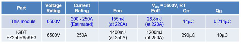
Click image to enlarge
Table 3: Comparison of losses between the Supercascode module and IGBT of similar rating. The Supercascode can clearly be used at 10X higher frequency given the low switching losses
Applications of HV switches: Medium Voltage Solid-State transformers
A solid-state transformer generally takes a medium or HV AC input, say 4160V AC, 13.8KVAC, and transforms it into a lower voltage output, without the use of a bulky 60Hz transformer. The basic concept is shown in figure 5, where AC voltage is first rectified, then converted to a high-power, high frequency AC in the 5-100kHz range. A much smaller mid/high frequency transformer provides a reduced secondary voltage, which can be rectified to provide a low voltage DC bus. This voltage can then be used to charge a car, or a drive a DC-AC inverter to manage lower voltage motor loads. The solid-state transformer is generally a fraction of the size of a 60Hz transformer, allowing the distribution of power to occur at very high voltages, and conversion to lower voltages being done at the point of use. This reduces the current at which power is distributed, reducing copper weight and cost, and reducing losses. This can be particularly useful at megawatt power levels, as in DC fast charging stations that need to charge 8-10 cars at 250-350kW, or on large ships to reduce copper losses that occur when distributing lower voltage AC.
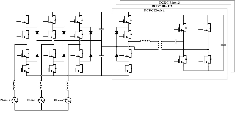
The primary side rectified voltage is >6KV and if switching frequencies above 500Hz-1KHz are needed, one cannot use 3.3KV-6.5KV class IGBTs or IGCTs. Instead, users may elect to use a multi-level inverter architecture with 7+ levels of 1700V IGBTs, or a modular multi-level converter (MMC) with many cascaded, lower voltage converters timed to provide a stepwise sinusoidal output. An example of a modular multi-level converter is shown in figure 6, where each stage of the converter uses a 3-level 1700V IGBT module on the primary side. Figure 7 shows a 3-level SiC implementation with 10KV switches. Clearly, the SiC implementation goes a long way to simplifying the architecture and control of such a DC-AC converter and can be operated at relatively high frequencies.

Click image to enlarge
Figure 6: Silicon based implementation of a modular multilevel converter system to implement a solid-state transformer (Huber et. al. ETH Zurich). Each of the cascaded converter cells has within it a 3-level 1700V module on the primary. All these switches and all these converters then need to be controlled to provide the desired output sinusoidal waveform
Click image to enlarge
Figure 7: A much simpler implementation using HV SiC MOSFETs or Supercascodes. The control complexity, and number of high voltage devices is much reduced. In order have a small transformer, switching frequency must now be 10X of the Silicon solution, and losses must still be kept manageable so as not to complicate thermal management. This is exactly where HV SiC devices excel
Megawatt class motor drives
An examination of the use of electricity in the US compiled by the DOE shows that 14% of all generated electricity is consumed by MW class industrial motor drives. Significant operating cost savings can be obtained by using these motors with variable speed drives instead of direct grid connection. These motor drives necessarily operate from higher bus voltages, in order to reduce operating currents to manage copper size and losses. Instead of using Si based inverters that operate at 500Hz-2kHz, SiC based inverters can be used at 10X higher frequencies, with much reduced cooling needs and system size.
The system designer has a choice of the same multi-level converter architectures using silicon as described in the last section, or a simpler 2-level or 3-level solution using SiC modules. It is also possible to raise the operating voltages with SiC which can reduce costs upstream from generation and distribution. Significant development is, however, needed with motor design and technology to fully exploit SiC capability. But even today, the benefits of SiC in improving motor operating efficiency by producing reduced current ripple, and inverter efficiency by cutting losses is well understood. In some applications, the use of SiC allows the use of higher RPM motors much smaller in size, and the possible elimination of the gear box.
Auxiliary power in high voltage systems
All the systems described above require operating low voltage power for the system control electronics (+/-5V, 12V, 24V), as well as for smaller auxiliary lighting and cooling systems. Smaller current rated modules with high voltage capability can help simplify the task of generating this power from the available medium voltage AC. This is an excellent application space for the Supercascode concept due to the ability to scale up voltage for the switches easily. One can also utilize the normally-on nature of the SiC JFETs in series with the low voltage normally-off MOSFET to simplify the start-up circuitry as has been demonstrated in low power flyback converters. Depending on the power level, users can choose between using power modules, or simply creating a PCB-based assembly using off-the-shelf JFET components.
HV DC Breaker
With the proliferation of DC based power generation and DC loads, fresh attention has been focused on how to use solid-state circuit breakers to replace mechanical breakers to enhance reliability, shrink size, reduce arc-flash concerns and add intelligence to the system protection. Since the solid-state breaker has no moving parts, and does not seek to disconnect a current mechanically, it is not subject to arcing concerns or mechanical wear of contacts. The main value of the solid-state approach to breaking DC current without forcing a resonant zero current crossing is that it can be done within 1microsecond with ease. Subsequently, a much smaller disconnect switch can be opened at zero current to provide galvanic isolation. This method dramatically reduces the duration and magnitude of fault current the downstream circuit and the source have to deal with.
Figure 8 shows an example of the type of arrangement typically used with a solid-state circuit breaker with bi-directional capability. Since the cabling and load inductance can vary widely in a large-scale power system, the stored energy in the line inductance must be dissipated when interrupting the DC fault current. This energy can be very large and is therefore absorbed by the MOV used in parallel in figure 8. The snubber elements moderate the dV/dt and di/dt during turn-off.

Click image to enlarge
Figure 8: Implementation of a bi-directional solid-state DC circuit breaker. The back to back switches provide the standoff voltage in either direction. The RC snubbers moderate the switching voltage transitions. The MOV is sized to absorb the worst-case stored energy in the line inductance. With the Supercascode switch, virtually any voltage or current handling level can be achieved
The main requirements for the switches used in this application is low conduction loss, easy voltage and current scaling, and robust operation under high fault current turn-off. The Supercascode approach again becomes beneficial here. SiC JFETs have a strong positive temperature coefficient of on-resistance, with nearly flat VTH versus temperature, and therefore parallel very easily, making high current scaling quite straightforward. And with the Supercascode technique, voltage scaling also becomes easy with just a single common source referenced low voltage MOSFET being driven to control the breaker operation.
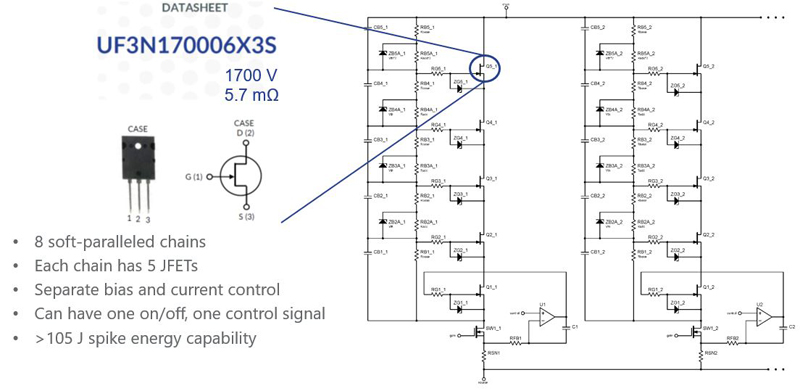
Using the Supercascode with a simple op-amp circuit alongside a low voltage MOSFET, as shown in figure 9, allows the implementation of a fast-acting current breaker with very low insertion loss, while also minimizing the peak fault current. This type of circuit can be modified to manage inrush current and only trip in the event of a real fault. In this example, voltage scaling is done by the series connected devices, while current scaling is done with the paralleled stages.
Click image to enlarge
Figure 9: A design example of a 6500V, 1000A current limiting circuit breaker. Comprised of paralleled 8 paralleled strings, each with 5 series connected JFETs. The trip current can be set using the voltage reference at the op-amp. Current can be sensed either as shown, or by using the VDS(ON) of the low voltage MOSFET
Conclusions
SiC devices are excellent candidates to improve power electronics in the medium and high voltage application space. From solid state transformers to megawatt class motor drives, auxiliary power systems to solid state circuit breakers, we have shown how SiC MOSFETs in general, and the SiC JFET-based Supercascode in particular, offer very compelling high performance and system simplification advantages. Growth in these applications will drive SiC-based power electronics growth in the future, well beyond the EV boom of the 2020s.
UnitedSiC