Automotive USB 2.0 and a 5 V, Type-C Solution for Charging
USB charging ports in modern vehicle infotainment systems face a variety of system challenges with respect to power, data transmission support, and robustness
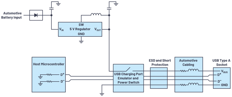
Figure 1. Automotive USB charger block diagram
USB charging ports have become an essential part of the modern vehicle infotainment system. Passengers are increasingly accustomed to connecting their vehicle’s electrical system to both power their portable devices and, conversely, use those devices for a variety of vehicle information and entertainment functions. To support both power and data capabilities, and to enable adaptability in continuously fast-changing portable device markets, USB charging ports must meet a variety of system requirements with respect to power, data transmission, and robustness in the face of real-world hazardous events.
Portable device battery charging—including the ability to support a wide variety of device charger profiles such as USB BC 1.2 charging downstream port (CDP), dedicated charging port (DCP), standard downstream port (SDP), and common proprietary profiles—is only one part of a wide range of demands placed on USB charging ports. Other requirements include maintenance of signal integrity for high speed USB data transmission, and USB host protection from hazardous conditions commonly found in the automotive environment. In addition, small solution size and low electromagnetic emissions are important requirements for meeting the demands of increasingly complex automotive electronics.
Automotive USB Power System Overview
Figure 1 shows a block diagram of a typical automotive USB charger system, in which a switching regulator generates 5 V from the battery to power VBUS. The USB charging port emulator plus power switch IC shown here has three main functions. First, the USB charging port emulator determines an attached device’s optimal charging current, enabling fast charging via charging port modes such as USB BC 1.2 CDP, DCP, and vendor-proprietary charger emulation profiles. Second, the USB power switch acts as a current limiter and switch, sensing and limiting the bus current. Finally, the port controller supports USB 2.0 high speed data transfer between an attached device and the USB host.
Since USB ports exist in a harsh automotive environment, sensitive USB circuits must be protected from a host of real-world hazards, such as electrostatic discharge (ESD) events at the socket and cable fault events, which can expose affected wiring to voltages well beyond their normal operating values.
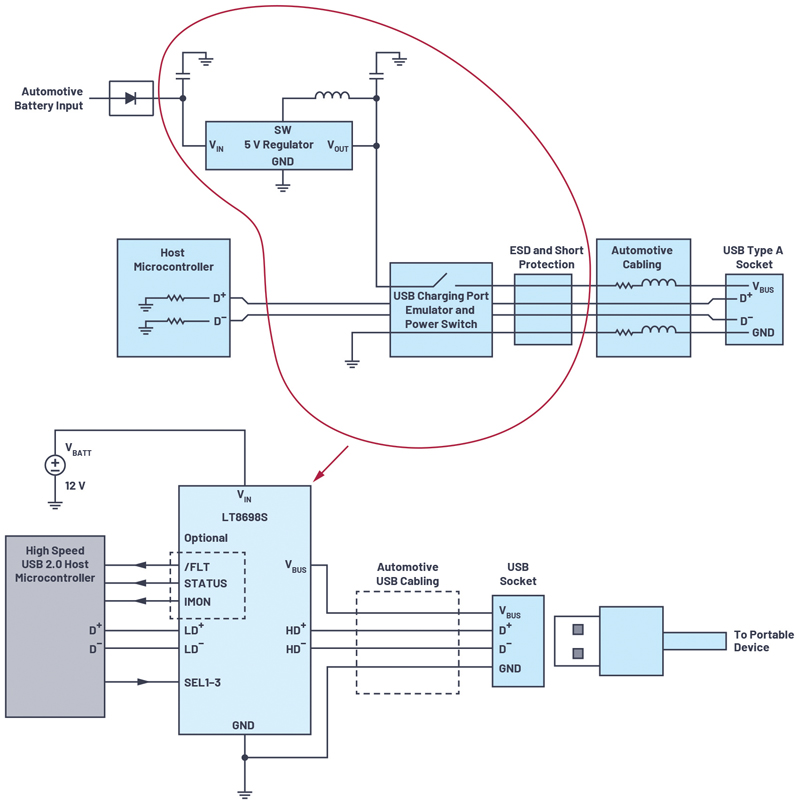
Figure 2 shows a simplified block diagram of an automotive USB power system that combines many of the power, port, and protection functions into a single IC. In this case, the LT8698S integrates the functions of the switching regulator and power switch into a 4 mm × 6 mm package while providing robust data line protections against ESD events and cable faults.
Click image to enlarge
Figure 2. Simplified block diagram of an automotive USB power system built around a single-IC USB controller solution
With the integrated charger solution shown, all of the necessary hardware to independently perform the USB BC 1.2 CDP negotiation sequence between the USB port and the portable device is included, allowing CDP compliant devices to draw current up to 1.5 A from VBUS while simultaneously communicating with the host at high speed.
Cable Drop Compensation
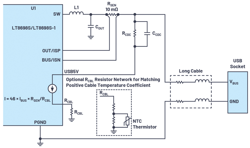
Cable drop compensation maintains accurate 5 V regulation of the VBUS rail when the USB socket is physically distant from the controller—for instance, the USB socket is located in the rear of a vehicle and the USB host is in the dash. The LT8698S features programmable cable drop compensation to provide excellent regulation at the USB socket without the need for additional Kelvin sense wires.
Figure 3 shows how cable drop compensation works. A sense resistor, RSEN, is tied between the OUT/ISP and BUS/ISN pins in series between the regulator output and the load. The LT8698S develops a current source value of 46 × (VOUT/ISP – VBUS/ISN)/RCBL at its RCBL pin through the RCBL resistor to ground. This current is identical to the current flowing into the USB5V pin through the RCDC resistor tied between the regulator output and the USB5V pin. This creates a voltage offset across the RCDC resistor, above the 5 V USB5V feedback pin, and proportional to the RCDC/RCBL resistor ratio. As a result, the LT8698S regulates the BUS/ISN pin to a point, in proportion to the load current, above the at-the-load target 5 V (subject to a max limit of 6.05 V) to maintain accurate regulation at the socket’s VBUS pin.
Click image to enlarge
Figure 3. Working principles of cable drop compensation
Cable drop compensation eliminates the need to run an additional pair of Kelvin sense wires from the regulator to the remote load, but requires the system designer to know the cable resistance, RCABLE—the LT8698S does not sense this value. Components for programming the cable drop compensation can be chosen using the following equation: RCBL = 46 × RSEN × RCDC/RCABLE. Since cable resistance varies with temperature, to achieve better overall output voltage accuracy over a wide temperature range, cable drop compensation can be made to vary vs. temperature by adding a negative temperature coefficient (NTC) resistor as part of RCBL.
Robust Protection
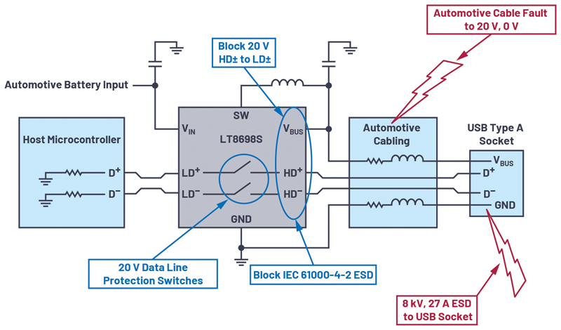
The automotive environment presents a number of hazards from which the USB host must be protected. These hazards include cable faults resulting in data line exposure to the battery voltage or ground, and large ESD strikes at the USB socket. Figure 4 shows how to protect the USB host from these hazards.
Click image to enlarge
Figure 4. Robust protection features of LT8698S/LT8698S-1
The LT8698S’s HD+ and HD– pins withstand up to 20 VDC and block up to 8 kV contact discharge and 15 kV air discharge IEC 61000-4-2 ESD events while simultaneously protecting the host from these severe conditions. In addition, the USB5V, OUT/ISP, and BUS/ISN pins withstand output voltage faults that include dc voltages up to 42 V. In the event of an output fault, the latch-off and auto-retry features accurately limit the average output current.
While many USB port controller ICs require external clamp diodes or capacitors on the data lines for ESD protection—increasing cost and material, while possibly degrading signal integrity—the LT8698S does not.
Despite the data line switches’ ability to withstand dc faults and ESD events as previously stated, they also support excellent signal integrity. Specifically, the –3 dB bandwidth of the HD+ and HD– pins is 480 MHz (typ), which is production tested.
A Wide Variety of Charger Profiles
The controller IC used in the examples here is compatible with a number of USB connector types and charger profiles. Let’s look at how a single controller solution might work in a USB type-C 5 V, 3 A solution (15 W).
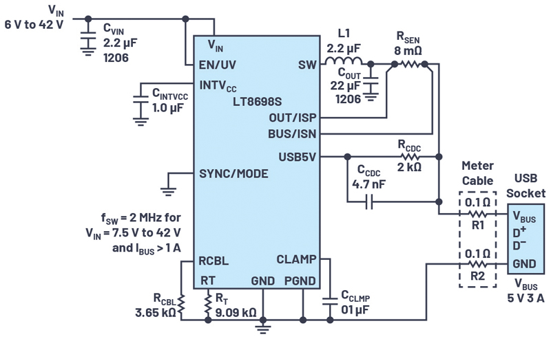
Figure 5 shows the schematic for a USB 5 V at 3 A VBUS regulator with cable drop compensation. In this circuit, the RSEN resistor value of 8 mΩ is chosen to support up to 3 A of current, and the SYNC/MODE pin is tied to ground to enable pulse-skipping mode of operation, reducing the switching frequency and quiescent current at light load currents.
Click image to enlarge
Figure 5. A 5 V, 3 A, USB type-C application
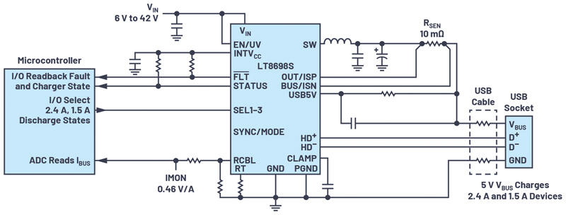
The LT8698S also supports USB BC 1.2 DCP mode, which can supply charging currents up to 1.5 A for high current charging capability. When used as a DCP port, the D+ and D– lines are shorted together and there is no data transfer. Many portable device manufacturers have developed proprietary charger protocols. In addition, these vendor-proprietary charger profiles and associated maximum charge currents, such as 2.0 A, 2.4 A, 2.1 A, and 1.0 A, are supported. The host microcontroller can implement these charger profiles by controlling the three SEL pins.
Figure 6 shows the schematic for a 2.4 A/1.5 A USB charger. In this application, the microcontroller utilizes the information provided by the LT8698S STATUS pin and IMON current monitor to select the desired charger profile by controlling the SEL1–3 pin input pins. In this way, the microcontroller can optimize the charger profile to the portable device for safe charging at the highest possible current.
Click image to enlarge
Figure 6. A 2.4 A/1.5 A automatic profile detection charger with current monitor
EMI
Low EMI is a key requirement for power supplies in automotive electronics systems, which are often expected to meet the CISPR 25 Class 5 emissions standard. The LT8698S is designed using Silent Switcher 2 technology, enabling the USB power supply to meet these stringent automotive EMI standards without sacrificing solution size, efficiency, and robustness.
Analog Devices


