Bringing WBG technology to the next level: Part 3 of 4 Editorial Series sponsored by Infineon: The fundamental game-changers for breakthrough SiC designs
Three essential aspects to consider when choosing the right SiC device for your next project
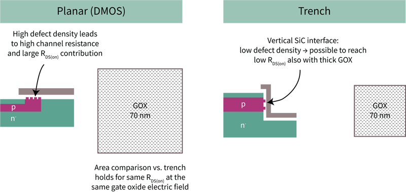
Figure 1. Comparison of planar and trench MOSFET structure
Introduction
Society’s demand for energy is continuously increasing. A plethora of digital content is consumed every day, appliances are connected via the cloud, and vehicle electrification is experiencing a renaissance – all of which are contributing to this energy demand upsurge. At the same time, carbon emissions need to be reduced, which makes it necessary to generate and consume energy sustainably. One way to live up to this growing demand for more green energy is the use of highly efficient power conversion designs based on silicon carbide (SiC) power semiconductors.
There are plenty of choices in the market when it comes to power semiconductors based on SiC. Regardless of their selection, designers can reap the inherent benefits of SiC, such as enabling higher switching frequencies, high efficiency, and reduced heat dissipation. However, it is worthwhile to take a closer look at additional features that translate into design and system benefits, as they can lead to significant cost savings. Considering the device design, the right synergy between the chip and its package, as well as strategic aspects regarding manufacturing and capacity, really pays off.
Device design – pioneering in trench SiC MOSFETs
Infineon is a pioneer in trench SiC MOSFET technology reaching back to first publications already in the 90ies [1]. This deep know-how of the limits and possibilities and the quality of Si-MOS technologies was fundamental to deciding on a trench-based device concept (Figure 1). The trench SiC MOSFET allows users to reap the benefits of low on-state resistance without compromising reliability. Generally, trench-based vertical power devices enable the best material utilization in the form of small die sizes for a given performance, as recognized by the historical development of silicon-based power switches. This is especially relevant for SiC components since the material itself is a strong cost driver.
Furthermore, due to the specific physical characteristics of the SiC crystal in trench-based devices, a lower area-specific resistance can be achieved compared to devices with planar configuration if safe operating electric fields for the gate oxide are maintained. Thus, the trench MOSFET concept provides the opportunity to combine reliability with outstanding performance. Additional benefits like sufficiently high threshold voltage, adjustable short circuit ruggedness, attractive avalanche ratings, and favorable capacitance ratios enable low-loss, rugged and simple converter designs.
Another feature that comes from the device design is the intrinsic body diode in SiC MOSFETs, which eliminates the need for an external fast freewheeling diode. Infineon’s CoolSiC™ MOSFET allows the full utilization of the body diode, resulting in high robustness under hard commutation and low reverse recovery. Technological measures and screening procedures ensure that active body diode operation does not lead to critical drift effects.
A trench-based SiC MOSFET can be designed with a high threshold voltage, being a benchmark for a robust signal-to-noise ratio during current turn-off. This is crucial for implementing zero gate-voltage turn-off similar to Si MOSFETs at the system level. Zero voltage turn-off simplifies the gate driving scheme, as no negative drive voltage is needed. This leads to higher system reliability by reducing part count and complexity.
The challenge of a zero-voltage turn-off is basically the unwanted parasitic turn-on effects. Since a MOSFET could be represented as a capacitance divider, any drain-source voltage change will result in a gate-source voltage change. If the gate-source voltage is higher than the MOSFET threshold voltages, the MOSFET will turn on slightly, which will increase the turn-on losses.
CoolSiC™ MOSFETs are robust against parasitic turn-on due to:
- increased threshold voltage; Infineon CoolSiC™ technology holds the benchmark in high threshold voltage
- optimized capacitance ratio to minimize the unwanted voltage coupled from the drain-source voltage change.
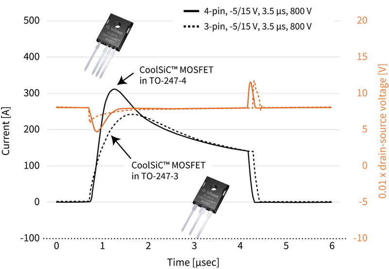
Infineon´s trench technology provides a low on-resistancecombined with a short-circuit capability. Depending on product configurations for specific target applications, Infineon’s CoolSiC™ MOSFET products specify a short circuit withstand time of up to 3 μs. Drive-type applications require, in general, short-circuit capability. The example in Figure 2 shows the short circuit behavior for a 1200 V discrete MOSFET. If the short circuit withstand time is specified in the datasheet, it is mandatory to implement measures to ensure that the production parts cohere to this performance. Infineon is handling this by performing a 100 percent production test on all products with specified short circuit withstand time prior to shipment.
Click image to enlarge
Figure 2. Short-circuit behavior of Infineon’s 1200 V CoolSiC™ MOSFET in different package configurations (with and without source sense)
Synergies between the chip and its package
Compared to silicon (Si) chips, SiC-based chips are smaller in size. What may seem to be a trade-off in terms of thermal performance and power handling capability, can be mitigated by using sophisticated interconnect technologies to reach the highest utilization of the material. The CoolSiC™ chip technology is therefore combined with suitable discrete and module packaging to boost the thermal performance of the devices.
For discrete devices, a diffusion soldering method is used. The main advantage of using diffusion soldering is the significant reduction of the device’s thermal impedance. In contrast to the usual die-attach technology, which uses a solder layer between the chip and the package, the new solution is enabled by a special metal layer on the die backside, which forms the mechanical and thermal connection, as shown in Figure 3.

Click image to enlarge
Figure 3. Comparison of standard and diffusion soldering methods: Standard soldering (left) vs. .XT interconnection with the virtual elimination of solder joint through diffusion soldering
The reduction in thermal impedance results in higher power density. The static value (RthJH) improves about 25 percent, while the thermal impedance (ZthJH) shows an improvement of about 50 percent at 10 ms.
Moreover, diffusion soldering provides additional benefits for the application in terms of reliability. Since for a given total loss, the device will remain cooler than with standard solder, effects like bond wire lift-off can also be suppressed, and thus, higher cycling stability is achieved.
Power modules packaging differs substantially from their discrete counterparts. It has turned out that the perfect match to the SiC chip properties is offered by flexible pin-based configurations like the baseplate-free EasyPACK™ platform invented by Infineon decades ago.
Infineon’s EasyPACK™ modules combine perfect ingredients for connecting SiC chip performance to the system. First of all, the topology and internal layout can be very flexible due to a dense grid array for potential terminal positions, equipped with a highly reliable pin-rivet connector system. This technology enables low inductance in the gate- and power loops, especially if the modules are inserted into multi-layer power PCBs (see Figure 4).

Click image to enlarge
Figure 4. FF11MR12W1M1_B70 [3] with laminated PCB
Of equal importance is the thermal performance of the module, which is described for an EasyPACK™ module by the thermal resistance from the junction to the heatsink (RthJH). Infineon recently launched EasyPACK™ modules with aluminum nitride (AlN) ceramics. These modules show a 40 percent lower RthJH compared to conventional materials. The thermal benefit can be translated into various advantages on the system level.
Figure 5 compares a conventional EasyDUAL™ 11 mΩ/1200 V half-bridge module and an AlN version. The results show that with the AlN version, it is either possible to decrease the junction temperature by ~20 K or to increase the output current by ~30 percent.
A lower junction temperature would lead to improved efficiency and an extension of the lifetime with regard to power cycling. In contrast, higher output currents consequently lead to higher output power ratings.
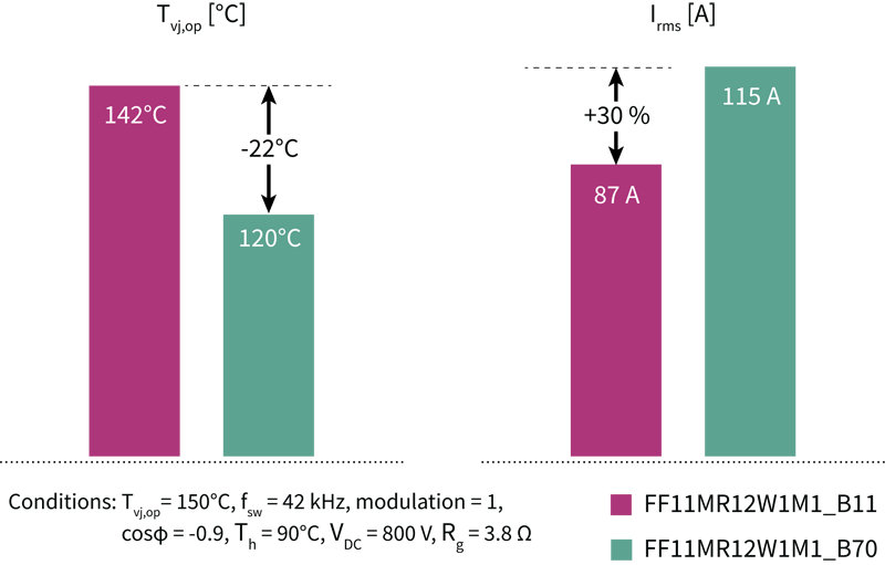
Figure 5. Benefits of AlN ceramics, conventional (FF11MR12W1M1_B11 [2]) vs. AIN (FF11MR12W1M1_B70 [3])
Manufacturing know-how
The established production flows at Infineon aim at high volume and high flexibility for both Si and SiC chip manufacturing, as well as for assembly into discrete packages or power modules. This is proven by the successful ramp-up of several advanced Si device technologies such as CoolMOS™ and TRENCHSTOP™ IGBT. Since 2001, also commercial SiC devices have been produced in high volume in an industrial environment – using the same tools and quality measures as applied for silicon power technologies
Scalable production processes combined with zero-defect strategies are the key to success and are well recognized by our customers. Infineon keeps key technologies like epitaxial growth and advanced packaging in-house. The long presence in the field helped us to develop dedicated quality assurance procedures covering typical SiC-specific aspects in production and in the field. Recently, Infineon announced the next great strides in driving SiC toward the mainstream by investing 2 billion € in wide bandgap (WBG) capacities in Austria and Malaysia [4].
Conclusion
SiC has evolved from a niche technology towards becoming a widely-accepted power semiconductor material. Deep manufacturing know-how based on a proven track record in the market has become as vital as the chip performance itself. This article presented three key aspects that need to be considered when developing highly efficient SiC designs. Infineon’s pioneering trench technology in the device design, the offering of the right synergy between the chip and its package, and finally, the company’s strategic aspect regarding manufacturing and capacity promise to cater to designers’ needs for unmatched reliability, variety, and system benefits. All measures are paving the way for a bright SiC future.
To find out more about the CoolSiC™ technology, CoolSiC™ products, and CoolSiC™ for systems, click here.
References
[1] D. Peters et al., “An 1800 V triple implanted vertical 6H-SiC MOSFET,” IEEE Transactions on Electron Devices, Volume: 46, Issue: 3, 1999
[2] Infineon Technologies, “FF11MR12W1M1_B11, v2.2”, Datasheet, July 2018.
[3] Infineon Technologies, “FF11MR12W1M1_B70, v2.0”, Datasheet, May 2020.
[4] Infineon Technologies AG, “Infineon doubles down on wide bandgap by investing more than €2 billion in a new Kulim, Malaysia frontend fab to expand market leadership in power semiconductors”, published 17 February 2022.


