For MOSFET reliability in flyback power supplies
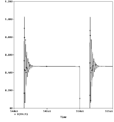
AC-DC power supplies up to approximately 100W commonly utilize the flyback topology. Its low cost and ability to provide multiple tracking outputs with a single controller have made it a favorite among designers and a de facto standard for low component count AC-DC converters. One disadvantage of a flyback converter is the high stress placed on the primary switching element. Flyback topologies operate by storing energy in the transformer during the on-time of the power switch and transferring this energy to the output during the off-time. A flyback transformer is comprised of two or more coupled windings on a core containing a series air gap across which (magnetizing) energy is stored until it can be transferred to the secondary. In practice, the coupling between the windings is never perfectly matched, and not all of the energy is transmitted across this gap. A small amount of energy is stored within and between the windings in what is referred to as the leakage inductance of the transformer. When the switch opens, the energy in the leakage inductance is not transferred to the secondary, but instead generates a high voltage spike across the transformer primary winding and the switch. It also results in high frequency ringing between the effective capacitance of both the open switch and primary winding, and the leakage inductance of the transformer (Figure 1).
If the peak voltage of this spike exceeds the breakdown voltage of the switching element, which is normally a power MOSFET, it can result in a destructive failure. Moreover, the high amplitude ringing on the drain node causes a significant amount of EMI. For power supplies above approximately 2W, a clamp circuit is used to limit the voltage spikes across the MOSFET by safely dissipating leakage inductance energy.
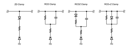
A clamp circuit is used to limit the maximum voltage across the MOSFET to a specified value. Once the voltage across the MOSFET reaches the threshold, all additional leakage energy is diverted into the clamp circuit where it is either stored and slowly dissipated or recycled back into the circuit. One disadvantage of a clamp is that it dissipates power and can reduce efficiency. For this reason, there are many different types of clamp circuits (Figure 2). Several use Zener diodes to minimize power consumption, but also increase EMI generation from the sharp turn-on of the Zener. The RCD clamp provides a good balance of efficiency, EMI generation and cost and, as a result, is the most common.
The RCD clamp operates as follows: Immediately after the MOSFET turns off, the secondary diode remains reverse biased, and magnetizing current charges the drain capacitance (Figure 3a). When the voltage across the primary winding reaches the output reflected voltage (VOR) defined by the turns ratio of the transformer, the secondary diode turns on and magnetizing energy is transferred to the secondary. Leakage energy continues charging the transformer and drain capacitance until the voltage across the primary winding equals the voltage across the clamp capacitor (Figure 3b).
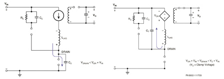
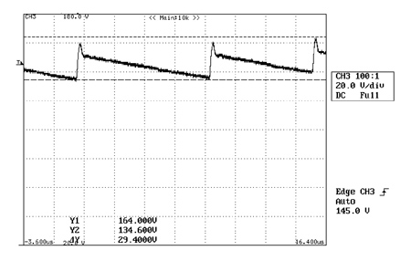
At this point, the blocking diode turns on and leakage energy is diverted into the clamp capacitor (Figure 4a). The charging current drawn through the capacitor clamps the peak voltage seen on the drain node to VIN(MAX) + VC(MAX). After the leakage energy is fully transferred, the blocking diode turns off and the clamp capacitor discharges into the clamp resistor until the next cycle (Figure 4b). A small resistor is often added in series with the blocking diode to dampen any ringing between the transformer inductance and clamp capacitor at the end of the charging cycle. This complete cycle causes the voltage ripple seen across the clamp circuit referred to as VDELTA, with the amplitude controlled by the sizing of the parallel capacitor and resistor (Figure 5).
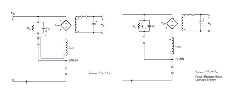
The RCDZ clamp is identical in operation to the RCD clamp except that the Zener diode in series with the resistor shares the dissipation (Figure 2). The Zener diode prevents the capacitor from discharging below the Zener blocking voltage. This limits power dissipation and improves efficiency, particularly at light loads. The ZD clamp provides a hard clamp of the MOSFET voltage specified by the blocking voltage of the Zener. Finally, the RCD+Z clamp operates in the same way as an RCD clamp, with the added Zener providing a fail-safe hard clamp for the MOSFET voltage during transient conditions, along with the EMI generation characteristic of the RCD during normal operation.
Clamp design must take into consideration the characteristics of both the transformer and MOSFET. If the minimum clamping voltage is below the VOR of the transformer, the clamp will act as a load, dissipating more than just leakage energy and reducing efficiency. If the clamp components are undersized, they may overheat, fail to prevent dangerous voltages and create unnecessary EMI. Most importantly, the clamp must protect the MOSFET under all conditions of supply input voltage, load current, and component tolerances. A Clamp Sizing Design Guide (PI-DG-101) published by Power Integrations, Inc., provides a step-by-step procedure for sizing components in each of the four major clamp type circuits for a flyback power supply. The Design Guide is intended to be used together with PI Expertä design software. PI Expert is an interactive program that takes a user's power supply specifications and automatically determines the critical components (including transformer specifications) needed to generate a working switch mode power supply. PI Expert will create a clamp design automatically, but the result will be slightly more conservative than that generated by following the algorithms in the Clamp Sizing Design Guide.
Below is a summary of the steps to follow when designing an RCD clamp. For complete details, please refer to the Clamp Sizing Design Guide. All values mentioned below not measured or defined by the user should be found in the PI Expert Design Results tab. 1. Measure the primary leakage inductance of your transformer, LL 2. Check the switching frequency of your design, fs 3. Determine the correct primary current, IP, as follows: a. If your design uses power limit programming, IP = ILIMITEXT b. If your design uses external current limit programming, IP = ILIMITEXT c. For all other designs, IP = ILIMITMA 4. Determine the total voltage allowed across the primary MOSFET and calculate Vmaxclamp as:
After the initial design, a prototype should be constructed to verify power supply performance, as transformer leakage inductance can vary significantly according to winding techniques. In particular, the average voltage Vclamp should be measured and compared with that calculated in Step 7 (Figure 5). Any significant deviation may be corrected by adjusting the value of Rclamp. If the results are significantly different from expected, the design must be iterated. The procedures for sizing the other clamp types follow the same process, with steps for each additional component. Care must be taken in diode and Zener selection to ensure their power ratings are not exceeded. In almost all cases where a Zener function is required, a transient voltage suppressor type should be used to provide the necessary instantaneous peak power rating. The power ratings of components should be verified by measuring body temperatures while the power supply is running at full load and lowest input voltage. If any component is operating above the manufacturer's recommended temperature limits, it should be resized and the design carefully evaluated against prototype results. Following the steps detailed in the Clamp Sizing Design Guide will result in a highly optimized and effective clamp design. Further information may be obtained and questions answered by posting an inquiry on the PI Power Supply Design Forum. www.powerint.com