Cost-effective dimmable CFL ballasts
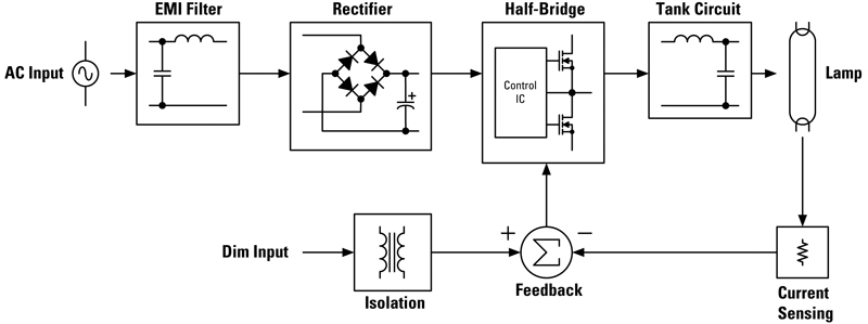
Figure 1: Dimming ballast block diagram.
Legislation mandating adoption of energy-saving lighting, such as the EU Lighting Directive, can help governments meet CO2 reduction obligations while also helping reduce end users' utility bills. As a consequence, Compact Fluorescent Lamps (CFLs) are becoming widely adopted, but their growing popularity is bringing demands for improved performance; in particular, the ability to dim CFLs easily and cost effectively. This article examines how software-based ballast design can help to meet these objectives. The Resonant Dimming Ballast Owing to the unique electrical behaviour and specification of CFLs, a dimming fluorescent ballast must integrate several important functions to manage start-up, running and dimming of the lamp. Figure 1 illustrates the main functional blocks.

The EMI filter, rectifier and smoothing capacitor convert the AC line input into a DC bus voltage and prevent ballast-generated noise entering the AC line. The half-bridge ballast-control IC produces a high-frequency square-wave voltage, which drives a resonant tank circuit for preheating, igniting and dimming the fluorescent lamp. This resonant half-bridge circuit allows a high voltage, up to several kilovolts, to be generated to ignite the lamp, and also ensures energy-efficient operation with low EMI through soft switching of the MOSFETs. Dimming is achieved by combining the fed-back current-sensing signals with the user-controlled dimming input to achieve the desired level of lamp dimming by adjusting the half-bridge frequency. The dimming input is usually galvanically isolated from the circuit. Figure 2 illustrates the operating points of the system during start-up and throughout the dimming range of the lamp. The circuit starts up at a high frequency, and then sweeps down towards the resonant frequency of the under-damped resonant curve, as described by the blue line. As the frequency sweeps down, the voltage across the lamp increases as the gain of the under-damped resonant curve increases. When the frequency reaches the calculated ignition frequency the voltage across the lamp will be approximately 750Vpeak and the lamp will ignite. This sequence helps avoid lamp flash by starting the lamp at a high frequency, and also allows for preheating of the lamp electrode, which extends lamp life. After ignition the resonant tank becomes damped due to the lamp resistance present in the circuit, and the system's behaviour follows the red line. The half-bridge controller IC closes the feedback loop and adjusts the frequency to somewhere between the 100% frequency and the 10% frequency depending on the desired dimming level. The resonant tank will become more or less damped as the lamp resistance increases or decreases during dimming (solid red line and dashed red line)
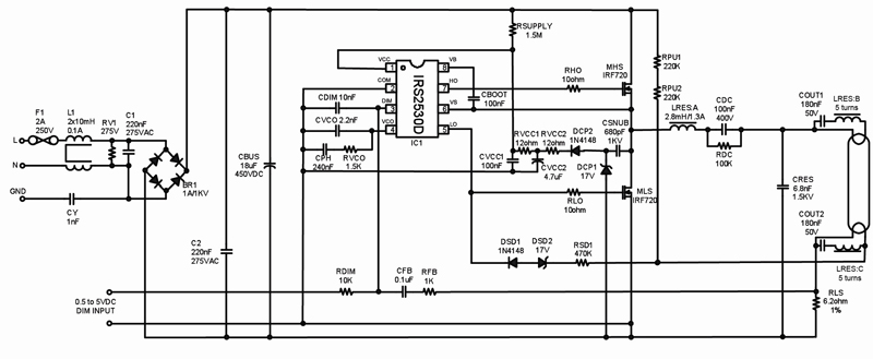
Speeding-Up Ballast Design PC-based design software such as IR's Ballast Design Assistant, IRPLBDA4, reduces the design time for electronic ballasts by helping to select a control IC, create a schematic, calculate component specifications and generate a bill of materials. The BDA also includes advanced simulation and analysis tools that enable designers to understand and optimise important parts of the ballast, such as the resonant tank circuit, to fine-tune ballast performance. The designer can quickly generate all the documentation needed to build the ballast by following a simple five-step procedure. This is readily accessible via the BDA's home screen, which presents clickable menu options that guide the designer through selecting the target IC, input circuit configuration, lamp type, and lamp circuit configuration. The fifth step is to click on the Design button to generate the schematics, bill of materials and inductor specifications. Advanced System Analysis This easy to use tool significantly reduces the time to design a dimmable CFL ballast. The key to improving ballast design, however, lies in knowing where the system's operating points are at all times. To assist with this, the BDA has advanced features that allow the designer to see, edit and fine tune the ballast and lamp input specifications, calculate the resonant tank components and view the circuit operating points graphically. This will give the designer a better understanding and feeling of how the circuit is working - in particular with respect to the resonant tank behaviour during the different modes of the lamp. Using the ballast and lamp data provided, the advanced screen shows values for the resonant tank components, displays the various operating frequencies that correspond to each lamp mode, and generates a Bode plot similar to that shown in figure 2 presenting a graphical view of the system's operating points. The BDA software also provides a ‘time domain' waveform viewer, which allows the designer to simulate switching waveforms to make sure the circuit is working as expected before building the actual circuit on the bench. When the input and output circuit parameters are acceptable, the designer can instruct the tool to generate a specification for the resonant inductor - including core type, core size, air gap, number of turns, and wire gauge - and to calculate the various programming resistors and capacitors around the chosen control IC. Clicking the Design button finalises the design and generates the complete set of output files for the ballast. Ballast Performance Figure 3 shows a complete schematic for a 26W ballast, as generated using the BDA. The half-bridge (MHS and MLS) is controlled by the IRS2530D dimmable ballast controller IC for preheating, igniting and dimming the lamp. Resistor RSUPPLY provides the micro-power start-up current for the VCC supply of the IC, and the charge pump (CSNUB, DCP1 and DCP2) takes over as the IC supply once the half-bridge begins to oscillate. CVCC1, CVCC2, RVCC1 and RVCC2 are used to filter VCC against high current spikes from the charge pump that can occur during hard-switching or inductor saturation. The resonant tank circuit (LRES and CRES) provides the necessary transfer function for generating high voltages for lamp ignition and low-pass filtering for dimming. A DC blocking capacitor (CDC) ensures that the lamp current is always AC to prevent mercury migration which can cause lamp-end blackening and shorten lamp life. Secondary windings from the resonant inductor (LRES:A,B) are used to heat the lamp filaments during preheat and dimming, and also separate the lamp current from the filament current. This allows for a single current-sensing resistor (RLS) to be used to sense the lamp current. The AC lamp current measurement across RLS is coupled to the DIM pin through a feedback capacitor and resistor (CFB and RFB). A DC dimming reference voltage is also coupled to the DIM through resistor RDIM. The resulting voltage at the DIM pin is the DC reference with the AC lamp current superimposed on top. As the DC reference is increased or decreased for dimming, the feedback loop of the IC keeps the valley of the DIM pin voltage regulated to COM by continuously adjusting the half-bridge frequency. This loop will then automatically increase or decrease the AC lamp current amplitude depending on the DC reference input voltage level. Finally, resistors RPU1, RPU2, RSD1, DSD1 and DSD2 are used to detect if the lamp has been removed and to restart the ballast automatically when the lamp is re-inserted. Protection against all other ballast fault conditions such as failure to strike, open filament, and low AC line/brown-out, are included internally to the IRS2530D. This further reduces component count and increases reliability. Conclusion This article has shown how software tools such as IR's Ballast Design Assistant simplify design and evaluation of dimmable fluorescent ballasts. BDA can be freely downloaded from the International Rectifier website at: www.irf.com . www.irf.com


