Compensating optocoupler feedback
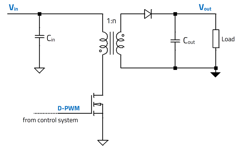
Figure 1: Power stage of the flyback converter (simplified)
Isolated flyback converters often use optocouplers in the feedback loop to regulate the output voltage. As part of the compensation circuit, its parameters such as CTR influence the control loop and must be taken into account in the flyback converter design.
The flyback converter is an isolated switching power supply topology that is often used for output powers below 150 W (Figure 1). It not only provides galvanic isolation between input and output, but also generates an output voltage that can be higher or lower than the input voltage. The range of applications is broad and includes not only offline AC/DC conversion and PFC (Power Factor Correction) stages, but also high-voltage and low-voltage DC/DC converters in virtually all industrial sectors. Some examples of applications include main and auxiliary power supplies for household appliances, battery chargers for smartphones and tablets, LED lighting, power supplies for desktop and laptop computers, Power over Ethernet (PoE), industrial power supplies, auxiliary power supplies in motor drives, etc.
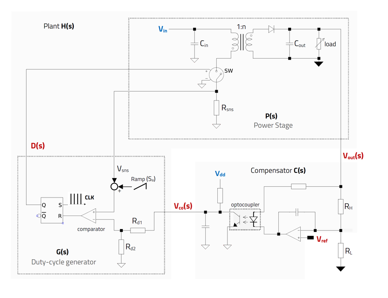
As with any isolated switching converter, the output voltage must be monitored to keep it at a target value even if the input voltage or output current fluctuates, and a corresponding signal must be fed back to the controller across the isolation barrier. The controller can then adjust the duty cycle of the control transistor (Q1) based on the feedback signal, thus regulating the energy flow from the primary to the secondary side to keep the output voltage constant. It is a typical closed loop negative feedback system where the unit (plant) consists of the duty cycle generator and the power stage, whose transfer function characteristics are defined by the design specifications, and a compensation block (compensator) required to "stabilize" and shape the dynamic response of the converter (Figure 2). The design of the compensation block is not only intended to ensure that the control loop is stable, i.e. that interference signals or transient events do not generate persistent oscillations in the system, but also that the output voltage after a transient event meets certain requirements in terms of overshoot and undershoot, ringing and settling time, the limits of which are usually specified by the connected load.
Click image to enlarge
Figure 2: Example of a flyback converter with isolated peak current control with optocoupler and op-amp feedback compensation (simplified)
In most isolated converters that require strict regulation of the output voltage, an optocoupler is typically used to transmit the output voltage feedback signal across the isolation barrier from the secondary side (compensation block) to the primary side (regulator). Optocouplers offer very high insulation voltage levels of over 5 kV as well as a mechanically robust insulation barrier with a small housing size, which helps the power supply unit to meet strict safety standards.
As the optocoupler transmits the feedback signal via the insulation barrier, it becomes part of the control loop - or more specifically: the compensation block. The compensation block must therefore be designed with the optocoupler's transfer function in mind. In particular, the current transfer ratio (CTR) of the optocoupler (with the corresponding fluctuations) and the parasitic capacitance between collector and emitter provide additional amplification/attenuation or phase shift of the feedback signal of the output voltage. If this is not taken into account, the stability of the power supply unit may be impaired and the transient response requirements may not be met.
Against this background, the application note ANP113 [1] from Würth Elektronik on which this article is based describes in great detail an example procedure for designing the compensation circuit of a flyback converter with current control and feedback on an optocoupler basis. It also contains the validation results in a prototype. Particular attention is paid to the design limitations caused by the parameters of the optocouplers and appropriate solutions are shown.
Stability analysis of the control loop
Figure 2 shows a flyback converter with its control loop. Note that the transfer functions are described in the Laplace domain s. The unit (plant) of the system with the transfer function H(s) is formed by the power stage P(s) and the duty cycle generator block G(s). It should be noted that the transfer function G(s) varies depending on the control method used, which leads to different characteristics of the unit for current and voltage control. The power stage transfer function P(s) is independent of the control technology. Figure 2 shows a simplified duty cycle generator block for a peak current regulator, as used in the example design described here. The compensation block shown is a type 2 compensator with operational amplifier and optocoupler circuit. Note that such a type 2 compensator can be implemented with different circuits and configurations. The most common are op-amps (operational amplifiers) such as the TL431 [2] (voltage reference with internal error amplifier, as described here) and OTA (operational transconductance amplifier).
Click image to enlarge
Figure 3: Block circuit of the control loop (unity-gain form) with transfer functions
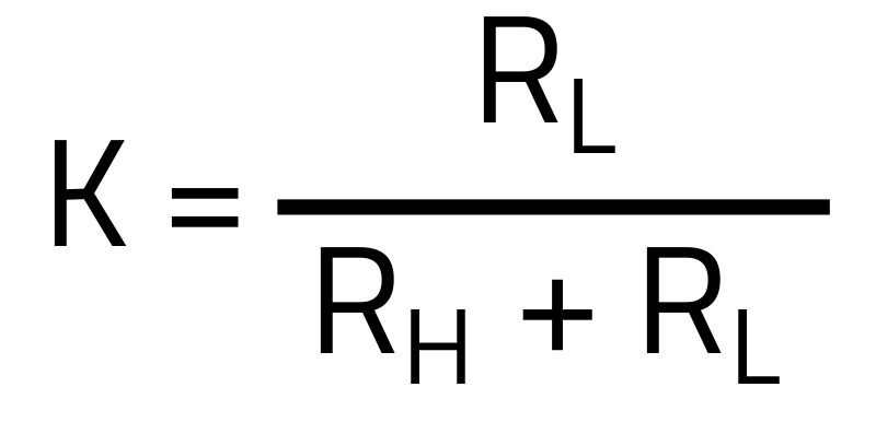
The circuit in Figure 2 can be represented as a closed-loop feedback system with transfer functions as in Figure 3. Figure 2 shows that the output voltage is reduced by a factor "K" by the resistor divider formed by RH and RL in order to reduce it for direct comparison with the reference voltage (Vref) at the input of the error amplifier (equation 1).
The transfer function of the closed control loop for direct current (s = 0) results from equation 2:
The advanced theory for estimating the phase margin and amplitude margin is explained in [1]. The same applies to the specific transfer function and the resulting requirements for the compensation block as well as the design of the appropriate compensation block with the TL431 voltage reference from Nexperia and the WL-OCPT optocoupler from Würth Elektronik (Figure 4).
Click image to enlarge
Figure 4: Type 2 compensation circuit with TL431 and WL-OCPT optocoupler
30 W flyback converter prototype
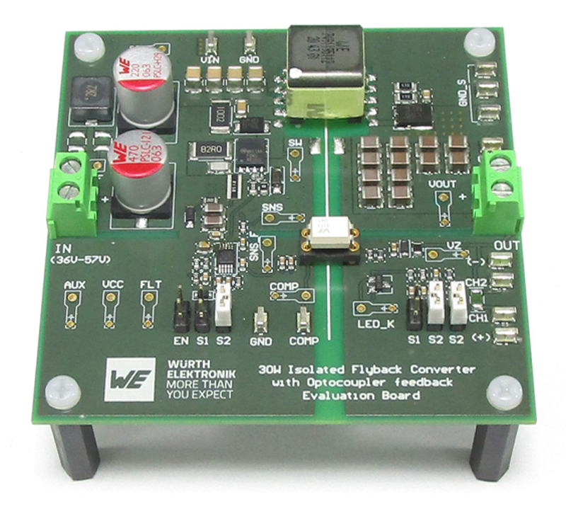
A 30 W flyback converter prototype was built with the following parameters (Figure 5):
The WE-PoEH 7491195112 [3] transformer from Würth Elektronik and the NCP12700 IC controller from onsemi [4] are used in the design. A WL-OCPT optocoupler from the 817 series and bin A with a static CTR of 0.71 at the DC bias conditions from [1, section 5.2] were selected for the measurements. It should be noted that the experimental results shown in this section apply to Vin_min = 36 V and full load Iout = 2.5 A. However, the stability of the feedback loop (phase and gain margins) must also be checked for all other expected operating conditions of the power supply and adjusted if necessary.
Click image to enlarge
Figure 5: Current-controlled flyback converter with optocoupler feedback loop
Measuring the frequency response
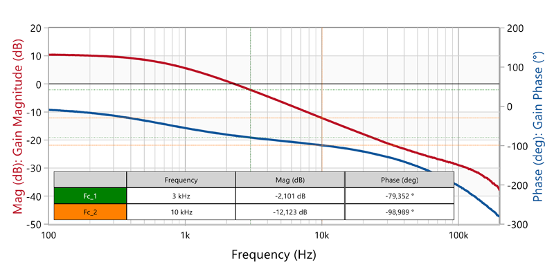
The transfer function between control and output shows a good agreement of magnitude and phase with the analytical results (Figure 6).
Click image to enlarge
Figure 6: Measured values for the unit: (control-to-output) amplitude and phase (Vin = 36 V, Iout = 2.5 A) (Bode100)
For 3 kHz, the analytical results showed a gain and phase of -2.1 dB and -82.4° respectively [1, Fig. 25], which is close to the measured values of -2.1 dB and -79.4°. For 10 kHz, the analytical results were -12.3 dB and -96.3° [1, Fig. 12], which is also a good approximation of the measured -12.1 dB and -99°.
The measured values for two different designs of the compensation block, the transient response of the load and the influences of the CTR variation of the optocoupler as well as the test setups are described in detail in [1].
References
[1] Falco, E.: Feedback loop compensation of a current-mode flyback converter with optocoupler, AppNote ANP113, Würth Elektronik: www.we-online.com/ANP113
[2] Voltage reference TL431 from Nexperia: https://www.nexperia.com/products/bipolar-transistors/3-terminal-adjustable-shunt-regulators/series/TL431-FAMILY.html
[3] Transforer WE-PoEH from Würth Elektronik: https://www.we-online.com/en/components/products/WE-POEH
[4] Current-mode PWM-Controller NCP12700 from onsemi: https://www.onsemi.com/products/power-management/dc-dc-power-conversion/controllers/ncp12700
[5] Optocoupler WL-OCPT from WürthElektronik: https://www.we-online.com/en/components/products/led/optoelectronic_optocoupler/wl-ocpt_optocoupler_phototransistor
