To reduce significant distribution losses due to high currents circulating on the Intermediate Bus in the Telecom/ Datacom distributed architecture, the value of this voltage (IBV) has been recently increased from the traditional 3.3V and 5V up to 15V.
If higher IBV brings evident benefits to the efficiency performance of the isolated 48V DC/DC Telecom Bus converter, especially in the case of unregulated IBV (see TI UCC28230) this creates significant challenges to the following PoLs. The efficiency of the PoL decreases drastically with the IBV value beyond certain points, due to the very narrow duty-cycle operation conditions. Therefore, particular effort has to be made to ensure that the achieved overall efficiency of the two stages of power conversion is indeed higher than before.
In this article, the challenges to be faced by the PoLs with this power architecture are investigated, through the synthesis of a complete design being carried out for an application in the Telecom arena.
Analysis, design of complete schematics and BOMs, together with prototype boards of the main three PoL converters required by the specific application, have been realized, to serve as hardware support tools for customers facing the challenges of increasing the Bus Voltage in their applications.
Power Converters Specifications
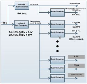
The analysis started from the initial power specifications, consisting in an Intermediate Bus Architecture, with an unregulated voltage swinging between 7V and 14V. This brings, according to the block schematic in fig.1 where the traditional architecture IBV is represented, the eventual simplification for the conversion to the 24V in a typical antenna line. In fig.1 efficiency values of the isolated DC/DC Bus converter vary from 92 to 95% with the swing of the output IB voltage. Power delivered by the IB will be P=280W, being 100W in the PoLs.
In this specific application, the main PoLs are:
- 0.7V.. 0.9V (VID) @ 6A (ASIC Multicore)
- 6.3V @ 4A (Low Noise RF Amplifier)
- 3.3V @ 16A (I/O)
In particular, the first conversion, extremely low output voltage (the ASIC adopts TI Voltage Identification Code to reduce the power consumption), highlights the challenge of the need to withstand a 14V maximum IB. The duty-cycle is down to 5% in that conditions, where the internal dead time of the PWM to be selected can play an unacceptable role. The second challenge is the efficiency, again due to the extreme operative conditions, especially for the Core and the I/O rails.
PWM selection
The new Texas Instruments PWM TPS4030x can withstand this critical application.
The part is 20V rated, which can withstand with a safety margin on the switching node (rated 27V) the input voltage plus the actual spike. TPS4030x provides feedforward compensation, useful in a non regulated IBA, to provide a fast response to input voltage changes. The device offers potentially very low on-time, down to typically 40nsec at 600kHz. Minimum duty-cycles can swing from 2.7 to 3.3% at 300kHz, 5.4 to 6.6% at 600kHz and 10.2 to 13.8% at 1.2MHz.
TPS4030x offers an accurate current source on its LDRV pin for over-current detection (integrated 3800ppm/C thermal gradient on over-current threshold delivers accuracy across the temperature range).
The application here calls for an increase in the switching frequency, to reduce dimensions and board cost, wherever possible according to the required minimum duty-cycle. Other best practices/ solutions implemented in the reference design boards, specific to the application, are:
- Where possible utilize ceramic as output capacitors, especially on the 0.7V, to achieve smaller voltage ripple.
- 3% output voltage step load transient to +/- 50% of full load.
- Dynamic VID, implemented by external 4-Bit signal driving an array of paralleled resistors, for output voltage swinging from 0.7V to 0.9V.
The very though dynamic specifications can be satisfied due to the capability of TPS4030x to achieve high cross over frequencies.
This is enabled by the characteristic of the Error Amplifier Gain-Bandwidth equal to typ. 20MHz Therefore just a couple of ceramic capacitors are sufficient and there is no need for high capacitance.
TPS4030x also presents strong output drivers (1.5/1.0 ohms (high side), 1.5/0.6 ohms (low side)), which help in minimizing switching losses and improve efficiency especially at high output current.
NexFETs Selection
To achieve the best overall efficiency with a minimum number of different NexFETs (TI's unique MOSFET technology for low capacitance and high switching frequency and power density), several calculations with varied bus voltages, switching frequencies and losses in the inductors have been done.
At the end all converters could be done with only two different NexFETs and two switching frequencies as shown below.
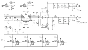
- 0.7V÷0.9V (VID) @ 6A fs=300kHz (TPS40303) PMP4709
- (Schematic in Fig.2)
- Inductor: Coilcraft MSS1048-222NLC
- 6.3V @ 4A fs=600kHz (TPS40306) PMP4711
- Inductor: Coilcraft MSS1260-682MLD
- 3.3V @ 16A fs=600kHz (TPS40306) PMP4713
- Inductor: Vishay IHLP5050FDEC1R05M01
- High side: CSD16409Q3 due to best overall performance (about 60mW losses, almost independent by Vin)
- Low side: CSD16323Q3 due to similar performance as CSD16340Q3 but better price (237 to 287mW, from 7 to 14V Vin)
The total dimension of PWM+FETs results in the compact size of 3x (3x3QFN) =27mm2
Therefore, in this specific application, the NexFETs have been selected according to the criteria of the smallest package/medium performance available. Indeed, the criteria can change from application to application, where power density, efficiency, thermal management and cost have to be leveraged to achieve the best compromise for the specific goals of the actual design.
To get the best flexibility inside the proposed boards, the PCB has been realized to accept different NexFET footprints. It is able to host both the SON5X6mm (compatibility with Power Pack for second sourcing), and the SON3X3mm. This makes it possible to test for every specific application different NexFET parts, according to the compromise requirement of performance/cost. As stated earlier, these kind of boards serve as a design aid to initial test of silicon in the specific application to customers, and it is the typical support (schematic, PCB layout, prototype board) being realized by the TI reference design team.
In this way, a Universal Demo-Board for TPS4030x, has been designed to be used in other projects, to also be able to propose different NexFETs with the two major sizes according to the required current/cost performance.
Measurements of realized converters
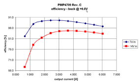
Efficiency measurements for one of the three converters is shown in fig.3, where testing was carried out for minimum and maximum IBV of the 0.7V.. 0.9V(VID) @ 6A ASIC PSU example.
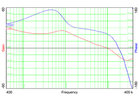
Open loop gain for the same converter is shown in fig.4, with evidence of the very high cross-over frequency obtained, about 100kHz, due to the excellent dynamic characteristics of the TPS4030x.
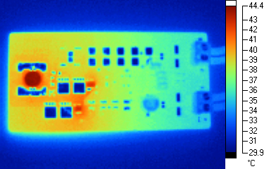
In fig.5, the thermal image of the board shows a maximum temperature of just 44.1 degrees, where the inductor and the high side and low side FETs have almost the same temperature.
www.ti.com