Integrated driver facilitates Class D amplifier design
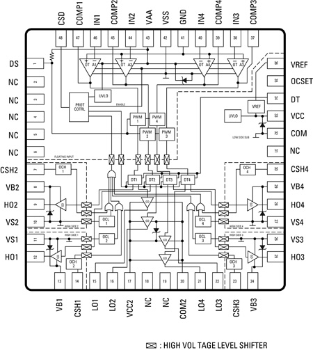
Whether it is automotive entertainment or home theater systems, consumers have been asking for more channels and speakers with the ability to handle higher audio power levels per channel. In addition to higher Wattage, the audiophiles have been demanding improved sound quality with lower distortion and noise, and excellent isolation between channels. In multi-channel design, driving each channel individually translates into higher power consumption, more components, and bigger board space resulting in a complex design with thermal issues, lower sound quality and reliability at higher cost. Thus, to minimize power dissipation and simplify thermal management of multi-channel high performance audio systems, designers have been tapping the benefits of high efficiency class D audio amplifiers capable of achieving efficiencies over 90% across a wide range of output power levels. By comparison, the efficiency of traditional class AB amplifiers serving this market is around 50%. And it falls rapidly as the output power level drops. Likewise, to cut component count and minimize board space, engineers have been exploiting the benefits of integrated ICs. Four channel driver Accordingly, blending advances in DirectFET power MOSFETs with an innovative integrated audio driver, International Rectifier has developed a four channel class D audio amplifier design that is comparable in performance to a single channel solution. To achieve that, this circuit utilizes an integrated audio driver, labeled IRS2093M, that packs four channels of high-voltage power MOSFET drivers on the same chip. In addition, the 200V device includes on-chip error amplifier, analog PWM modulator, programmable preset dead-time and robust protection functions specifically designed for class D audio amplifier applications in half-bridge topology (Figure 1). Aside from preventing shoot-through and rush of current through the power MOSFETs, the programmable preset dead-time also enables scalable power design both in terms of power and number of channels. The protection features include over current protection (OCP) with self-reset control and under voltage lock-out (UVLO) protection.
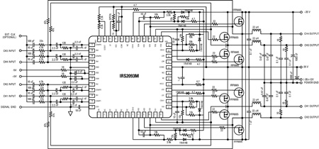
For excellent isolation between the channels, the audio driver implements proven high-voltage junction isolation techniques and floating gate drivers using Gen 5 HVIC process. As a result, there is excellent internal signal isolation on the die, enabling the circuit to process signals on more channels simultaneously. Thus, keeping the noise floor in each channel significantly low. And concurrently minimizing cross-talk between the channels. Subsequently, incorporating the integrated class D audio controller and gate driver IRS2093M along with eight DirectFET power MOSFETs IRF6665 and a few passive components, a four channel half-bridge class D audio amplifier circuit has been built as shown in Figure 2. Each channel in this multi-channel audio amplifier is designed to offer 120W output power. For ease of use, this circuit contains all the required house keeping power supplies.
To achieve best overall performance, the power MOSFETs IRF6665 have been specifically optimized for class D amplifier design. Besides offering low on-resistance, these power MOSFETs are also tailored for achieving minimal gate charge, body reverse recovery and internal gate resistance. In addition, the DirectFET packaging offers lower parasitic inductance and resistance as compared to conventional wire bonded packages. In short, IRF6665 MOSFETs are optimized for delivering high efficiency and low total harmonic distortion (THD) and electromagnetic interference (EMI). Features & Functions For achieving smaller space with highest performance and robust design, this four- channel class D audio amplifier solution employs self-oscillating PWM modulation. Since this topology corresponds to an analog version of a second order sigma-delta modulation with class D switching stage inside the loop, all the errors in the audible frequency range are shifted to the inaudible upper frequency range by the nature of its operation. The result is lower noise. Also, sigma-delta modulation permits a designer to apply a sufficient amount of error correction to further lower noise and distortion. As seen in figure 2, the self-oscillating topology comprises front-end integrator, PWM comparator, level shifters, gate drivers and output low-pass filter (LPF). Although, it can switch at much higher frequencies, this design uses 400kHz as optimum switching frequency for several reasons. First, at lower frequencies, the efficiency of the MOSFET stage improves but inductor ripple current increases, as well as output PWM switching carrier leakage rises. Secondly, at higher frequencies, switching losses degrade efficiency, but wider bandwidth is possible. While inductor ripple decreases, iron losses go up. Since in a class D audio amplifier the direction of load current alternates with the audio input signal, an over current condition can occur either during a positive current cycle or a negative current cycle. Hence, to protect both high-side and low-side MOSFETs against over current in either direction, the programmable OCP offers bidirectional protection. For that, it uses RDS(on) of the output MOSFETs as current sensing resistors. In this design, when the measured current exceeds the preset threshold, the OCP logic outputs a signal to the protection block, forcing HO and LO pins low, and thereby protecting the MOSFETs from damage. Due to the structural constraints of the high voltage ICs, current sensing is implemented differently for the high-side and low-side MOSFETs. For instance, low-side current sensing is based on the measurement of VDS across the low-side MOSFET during on-state of the device. To avoid triggering OCP from overshoot, a blanking interval inserted after LO turn-on disables over current detection for 450ns. The threshold voltage for low-side over current sensing is set by the OCSET pin, which is in the range 0.5 to 5.0V. Consequently, when the measured VDS of the low-side MOSFET exceeds the voltage at OCSET pin with respect to COM, the driver circuit begins the OCP protection sequence. To program the trip level for over current, the voltage at OCSET pin is calculated using the following equation. VOCSET = VDS(low-side) = ITRIP+ x RDS(on) In order to minimize the effect of the input bias current at OCSET pin, the resistor values R4 and R5 are selected such that the current through the voltage divider is 0.5mA or more. Also, using VREF to generate an input to OCSET through a resistive divider provides improved immunity from fluctuations in the supply voltage Vcc. Likewise, for positive load currents, high-side over current sensing also monitors the load condition, which is based on the measurement of VDS across the high-side MOSFET during high-side turn on via pins CSH and Vs. Subsequently, when the load current exceeds the preset trip level, the OCP protection shuts down the switching operation. To prevent triggering OCP from overshoot, a blanking interval inserted after HO turn-on disables over current detection for 450ns. Unlike low-side current sensing, the threshold for CSH pin is internally fixed at 1.2V. However, an external resistive divider R2 and R3 can be employed to program a higher threshold value. In either case, an external blocking diode D1 is used to block high voltages from feeding into the CSH pin while the high-side is off. Due to a forward voltage drop of 0.6V across D1, the minimum threshold for high-side over current protection is 0.6V. In short, the threshold value of the CSH pin, VCSH, can be calculated as: Where ID is the drain current and VF(D1) is the forward voltage drop of D1. Also, reverse blocking diode D1 is forward biased by a 10k? resistor R1. To prevent shoot-through or rush of current through both MOSFETs, a blanking period known as dead-time is inserted between either high-side turn-off and low-side turn-on or low-side turn-off and high-side turn-on. For optimized performance, the integrated driver permits the designer to select dead-time from a range of preset values, depending on the size of the MOSFETs selected. In fact, only two external resistors are required to set the dead-time via the DT pin of IRS2093. The end result is that there is no gate-timing adjustment required externally. Plus, it prevents outside noise from modulating switching timing, which is critical to audio performance. While determining optimal dead-time, the user must take into account the fall time of the MOSFET. This is because the effective dead-time in an actual application differs from the dead-time in the datasheet due to the switching fall time tf. That means, to determine effective dead-time, the fall-time of the MOSFET gate voltage must be subtracted from the dead-time value of the datasheet. Similarly, for UVLO protection, the driver monitors the status of voltage supplies VAA and VCC to ensure that both the voltages are above their respective thresholds before starting normal operation. If either VAA or VCC falls below the UVLO threshold, the protection logic of IRS2093 turns off LO and HO. As a result, the power MOSFETs are disabled until both VAA and VCC rise above their voltage threshold values. Furthermore, for optimum audio performance, the four channel audio board is designed to minimize trace impedances and curb coupling between analog and switching sections. Plus, it ensures that the analog signal ground is separated from the switching stage, as well as the power ground. Measured performance Using sinusoidal signal frequency of 1kHz at 1Vrms and 4? load impedance, efficiency, THD plus noise (THD+N) and EMI performance is measured on each of the channels. In addition, measurements were conducted to demonstrate the excellent isolation and cross-talk performance of the four channel class D audio amplifier design in figure 2. The supply voltages for the circuit board are �35V, while the self oscillating frequency is 400kHz.
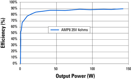
As illustrated in Figure 3, the efficiency per channel is about 90% from less than 50W power output to 120W output into a 4? load. Major factors contributing to high channel efficiency are low conduction and switching losses generated DirectFET MOSFETs IRF6665. And no cross conduction because of secure dead-time provided by the integrated driver. It is observed that with such high power efficiency, this four-channel design is able to handle one-eighth of the continuous rated power, which is generally considered to be a normal operating condition for safety, without any additional heat sinks or forced air cooling.
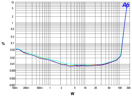
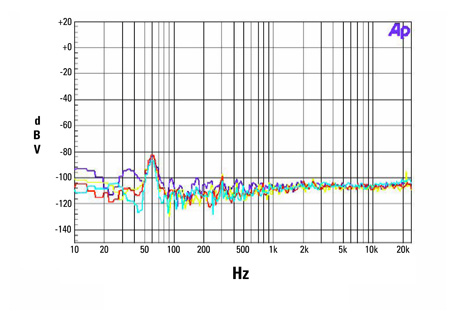
Similarly, tests conducted for distortion indicate that the THD+N performance for each of the channels is identical over a wide output power range. As depicted in Figure 4, the THD+N is less than 0.01% below 50W per channel and begins to increase as the output power increases. For instance, around 100W output per channel, the distortion rises to 0.02%. This performance remains consistent over the entire audio frequency range of 20Hz to 20kHz, even as the output power is enhanced from 10W per channel to 50W per channel with a 4? load. Likewise, as exhibited in Figure 5, the noise floor in each channel remains below -80dBv over the entire audio range. The noise is measured with no signal input and self oscillator at 400kHz.
Similar tests conducted for channel separation suggests that the cross-talk between channels 1 and 3 and 1 and 4 is better than -70 dB over the entire audio range at 60 W output power per channel. Also, this design offers good power supply rejection ratio (PSRR) of -68dB at 1 kHz signal. The high PSRR is the result of the self oscillating frequency of the driver. Thus, enabling the four-channel class D amplifier to deliver high performance even with the unregulated power supplies. Conclusions The efficiency, THD+N and EMI performance of this four-channel class D audio amplifier solution using integrated driver IRS2093M is comparable to single channel design. Additionally, the noise floor remains below -80 dBv over the entire audio range. And there is excellent isolation between the channels to keep intermodulation distortion (IMD) to a bare minimum for a satisfactory audio performance. While high efficiency eliminates heatsinks, the integrated audio driver realizes four-channel class D audio amplifier solution in a 50% smaller footprint. www.irf.com


