Challenges and trade-offs for portable electronics equipment
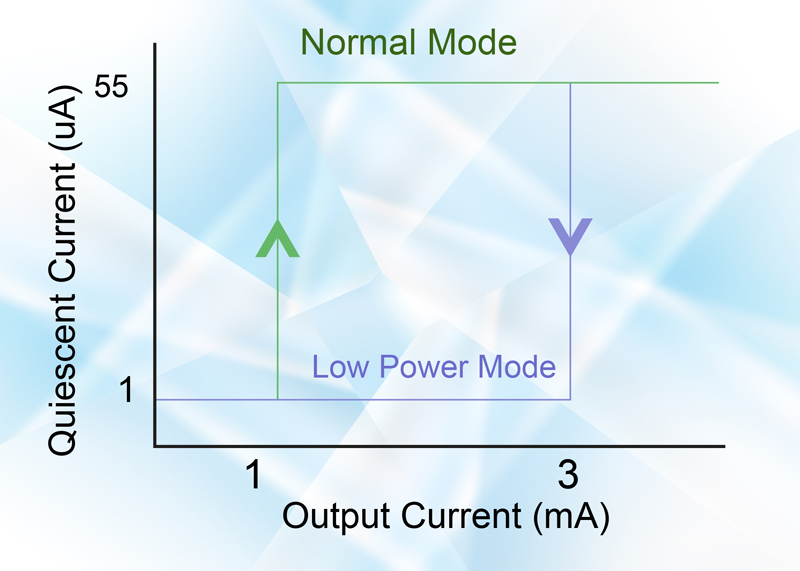
Figure 1: The challenge of dynamic performance vs. current consumption has been addressed by introducing parts that are switchable between low power mode and high performance. A typical example is ON Semiconductor's NCP4587.
Looking at products that are currently sampling, it appears that products with noise in the 10 ?VRMS range and Quiescent current in the 10-15 μA range will be in production by the end of this year, giving cell phone designers the best of both worlds in selecting their LDOs.
Low drop-out Linear voltage regulators are a vital component in a wide range of applications; perhaps some of the most demanding conditions exist in the portable equipment (media players, digital cameras, GPS systems, portable games consoles) and cell phone markets where the requirement to maximize battery life and to minimize size are just two of a number of factors that create tough challenges. Typically, the size issue has been addressed by using regulators in CSP or bump die form. However this raises challenges in terms of thermal dissipation and the assembly process. In addition, when creating an LDO regulator a designer traditionally has had to trade off current consumption against noise performance: unfortunately portable products demand both low power consumption and excellent ripple rejection and low noise generation. These challenges and numerous other trade-offs associated with the use of LDO voltage regulators in portable applications are discussed in detail in this article with the aim of providing valuable insight and information for design engineers tasked with designing next generation portable electronics equipment. Designing LDOs for the Portable Consumer market Standalone Linear Voltage regulators have always had an important, if somewhat unappreciated place in cell phones, their classic role being to isolate the RF section from the relatively noisy baseband chipsets. Rumors of their demise have abounded for years, with the assumption that increasingly, all embracing PMUs (Power Management Units) would supplant their necessity. However, the constant additions and changes of hardware features such as camera flashes, image sensors, Bluetooth modules etc. have continued to demand the flexibility (in terms of rapidly changing voltage and current options) and calming influence (electrically speaking) that only a discrete LDO can provide. With today's Smart phones, complex hinges and sliding panes have made the prospect of running all power rails from a single PMU unattractive, with the result that some of the more complex phones can have as many as five discrete LDOs, powering elements such as touch screens, keypads, image sensors and RF sections. Power Consumption vs. Noise Two of the most important features that designers have looked for in choosing LDOs for cell phones have been their dynamic performance and their size. In terms of their ability to reject external noise (as indicated by their Power Supply Rejection Ratio specification, which is measured in dB) and to avoid generating internal noise (usually stated in ?VRMS) it is interesting to look at the progression of LDOs for use in cell phones through the last 10 years. The earlier products were pure bipolar, with a typical PSRR of 45 dB and noise level above 30 ?VRMS. In order to achieve this noise specification, devices usually required a bypass capacitor connected to the internal Voltage reference of the regulator, a topology that became standard for low noise devices. A leap forward took place with the introduction of BiCMOS which is arguably still the benchmark for low noise LDOs in the wireless domain. A product specification with a typical PSRR of 75 dB (@ 1 kHz) and a noise rating of less than 10 ?VRMS was now achievable. Quiescent current remained and issue however with a typical 50 μA maximum consumption over all conditions. Just for reference, there are several CMOS devices on the market with Quiescent currents in the 1 to 4 μA range (at 0 load), but typically with poor Noise performance specifications. CMOS designers have tackled the challenge of dynamic performance vs. current consumption by introducing parts which are switchable between low power mode (with degraded dynamic performance but low power consumption) and high performance mode (good dynamic performance but at the price of higher current consumption). These modes can either be selected by the user, or automatically switched when the output load is very light. A typical example is the NCP4587 from ON Semiconductor, the performance of which is illustrated in figure 1.
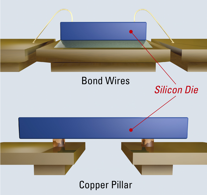
Size does matter The footprint of a CSP device matched the size of the actual die, without the need for space between the edge of a package and the die to allow for wire bonding. CSP tended to be very low profile (typically around 0.6 mm in height) making it very popular with manufacturers of portable consumer products. However, CSP is very sensitive to the material composition and the mechanical dimensions of the bump. CSP products typically have a die size of approximately 1mm by 1 mm. The bump size has been standardized to around 300 um, and a pitch between bumps of .5 mm .Most CSP products released today with four or five bumps tend to follow the standardized footprint. which effectively restricts them to a 1mm by 1mm footprint, with a typical height of 0.6 mm. The closest competitor to CSP packaging in terms of size has been DFN packaging (also known by the Amkor name of MLF). As the process of choice for LDO designs has migrated to a 0.25 or 0.18 micron process, the die size has been reduce to the point where, despite the need for clearance, the die can fit in packages as small as 0.8x0.8 mm. Whereas early DFN packages had heights around 1 mm, we now see the XDFN package with a height of 0.4 mm, considerable thinner than most CSP offerings. There are at least two bonding approaches being taken by manufacturers using small DFN packages (see figure 2). The first uses conventional wire bonding, relying on small die geometries to get die small enough to fit the package - as an example, to fit a 1.0 mm by 1.0 mm package, a die cannot be much bigger than 0.6 mm by 0.6 mm, depending on how aggressive the associated assembly site rules are. The second approach uses a standard flip chip approach using copper pillars instead of the conventional solder bumps. Copper pillars are grown on the die, which is then flipped over and attached via the pillars to the copper lead frame of the package. By eliminating the need for wire bonds, this approach allows for a bigger die size - a die close to 0.8x0.8 mm square can be accommodated in a 1x1 mm DFN package using this technique. This is an important difference in the cell phone space, where the sweet spot for output current for LDOs has moved from a 150 mA current output to a 200 mA output current. A majority of space on the die for any Linear Voltage regulator is taken up by the output power device so any technique that allows the use of a larger die size to help in power dissipation is useful. From the manufacturing standpoint, the cost saving of a smaller die is somewhat offset by the additional cost of the copper pillar process. From the designer's standpoint, in addition to die size, an interesting aspect is that of heat dissipation: which approach can dissipate the heat generated by the LDO in the most efficient manner? Adherents of the copper pillar approach claim that their approach is the most effective in transporting heat from the die surface, but most the packages used in the wire bond approach incorporate a small heatsink pad underneath the package which connects directly the substrate of the die to a heat pad on the PCB, providing a measure of heat transfer. It is difficult to find exact numbers as manufacturers tend to state thermal resistance numbers which are only valid under specific mounting conditions, but looking at datasheets of a part known to use copper pillars suggests a junction thermal resistance (?JA) for a 1mm x 1mm thin DFN 6 pin package of 150°C/W whereas values for more commonly available wire bonded products in a 1mm x 1mm thin DFN 4 are stated anywhere from 181°C/W to 250°C/W depending on the test PCB used. Based on this very narrow sample size, the advantage appears to go to the copper pillar approach, but not by much. With these developments in shrinking DNF packages, the decision to use CSP or packaged LDOs may soon be becoming a matter of choice rather than of necessity. It is interesting to note the introduction of the ultra think CSP, with a thickness of 0.28 mm, presumably for applications where the height profile of the package is of extreme importance, or where the LDO is going to be actually embedded in the PCB. Conclusion Choosing an LDO for a wireless application has usually involved making some decisions from the start: choosing between current consumption and dynamic performance, and between achieving the smallest footprint possible with a CSP package (possibly requiring some additional qualification testing, specialized manufacturing techniques or mechanical safeguards) or more traditional encapsulated packages with larger footprints. With the availability of small geometry BiCMOS processes tuned to Analog design requirements and of smaller, thinner DFN packages, more options are now open to designers of wireless circuit boards. www.onsemi.com


