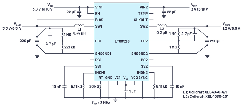
Figure 1. Ultralow EMI emission, dual output LT8652S-based 12 V to 3.3 V and 1.2 V synchronous step-down converter
Dual-Channel, 8.5 A, 18 V, Synchronous Step-Down Silent Switcher Device with 16 µA Quiescent Current
LT8652S is a dual-channel, synchronous, monolithic, step-down regulator featuring a 3 V to 18 V input range. It can deliver up to 8.5 A of continuous current from both channels and supports loads up to 12 A from each channel. It features peak current-mode control with an extremely low 20 ns minimum on-time, which allows high step-down ratios even at high switching frequencies. Fast, clean, low overshoot switching edges enable high efficiency operation at high switching frequencies, leading to a small overall solution size.
The LT8652S enables low EMI and a small solution size, a combination that few solutions can achieve. It features the proprietary Silent Switcher® 2 architecture, which minimizes EMI, while delivering high efficiency at high switching frequencies. In this architecture, the bypass capacitors are brought into the package, and by doing so, high di/dt loops are factory set in an optimized layout. Advertised EMI performance is easy to achieve since solutions are not sensitive to application layout. The LT8652S is a near turnkey solution for noise sensitive applications and environments.
For battery-powered applications, current draw at light load and no load idle is a critical parameter, as minimizing this current preserves battery run time. Idle conditions are where many applications spend most of their time. The LT8652S features 16 µA ultralow quiescent current under Burst Mode® operation, preserving battery life as long as possible. Integrated top and bottom N-channel MOSFETs contribute to impressive light load efficiency. The LT8652S also includes forced continuous mode that can control frequency harmonics across the entire output load range, with spread spectrum operation to further reduce EMI emissions.
The LT8652S offers both internal and external compensation options. Internal compensation yields smaller solutions by minimizing external components. External compensation via the VC pins enables fast transient response at high switching frequencies. The VC pins also simplify current sharing between channels for parallel, single output operation. CLKOUT and SYNC pins enable synchronizing other LT8652Ss to further expand current ability. To ensure tight output voltage regulation at the load for low voltage, high current applications, the LT8652S features a differential output voltage sensing function that allows Kelvin connections for output voltage sensing and feedback directly from the output capacitor.
In some high current applications, output current information is required for telemetry and diagnostic purposes. Limiting or derating the maximum output current-based on operating temperature may be required to prevent damage to the load. The LT8652S’s IMON pins can be used to monitor and reduce the load current. Load-based or board temperature-based derating can be programmed by using a positive temperature coefficient thermistor from IMON to GND. LT8652S can effectively control the load or board temperature by comparing IMON pin voltage with the internal 1 V reference. When IMON drops below 1 V, there is no effect.
Circuit Description and Functionality
A 3.6 V to 18 V input to 3.3 V/8.5 A and 1.2 V/8.5 A with 2 MHz switching frequency power supply is shown in Figure 1. Each channel can supply up to 12 Acontinuous load current. Only a few additional components are required for the complete solution, including inductors and a few passive components. Figure 2 shows that the circuit in Figure 1 achieves 94% peak efficiency.

Click image to enlarge
Figure 2. Efficiency vs. load current for LT8652S-based 12 V input to 3.3 V/1.2 V synchronous step-down converter
Differential Voltage Sensing Provides Tight Load Regulation
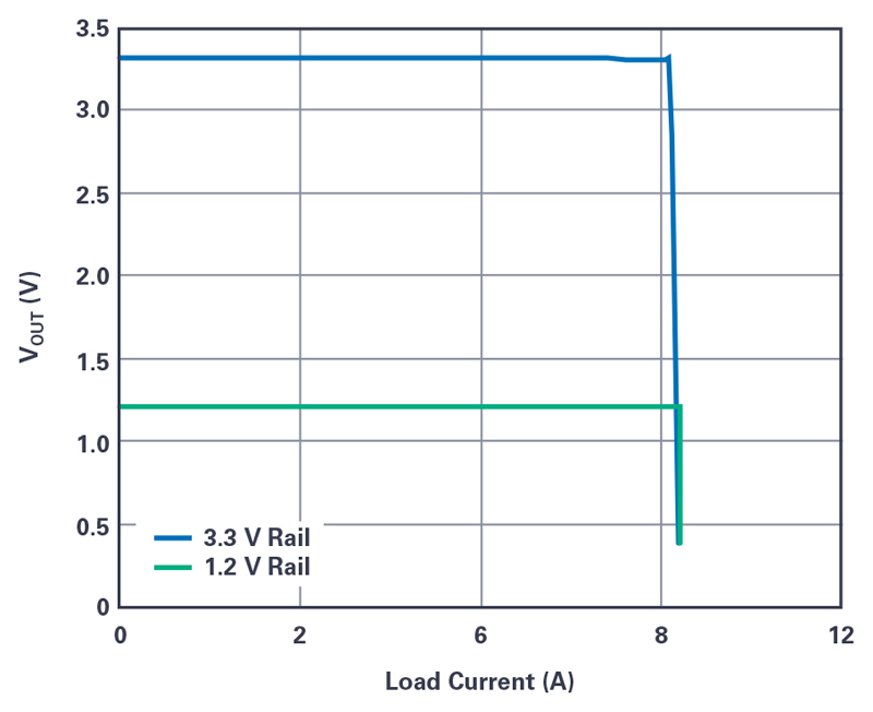
For high current applications, every inch of PCB trace incurs significant voltage drop. For low voltage, high current loads that require very tight output voltages, this voltage drop can cause serious problems. LT8652S features a differential output voltage sensing function, which allows the customer to make Kelvin connections for output voltage sensing and feedback directly from the output capacitor. It can correct up to ±300 mV of the output ground line potential. Figure 3 shows load regulation for both channels of Figure 1 using the differential sensing function.
Click image to enlarge
Figure 3. Load regulation and CVCC operation performance
High Switching Frequency with Ultralow EMI Emission and Improved Thermal Performance
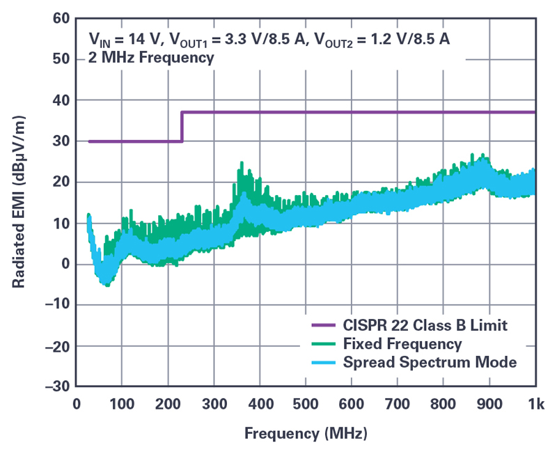
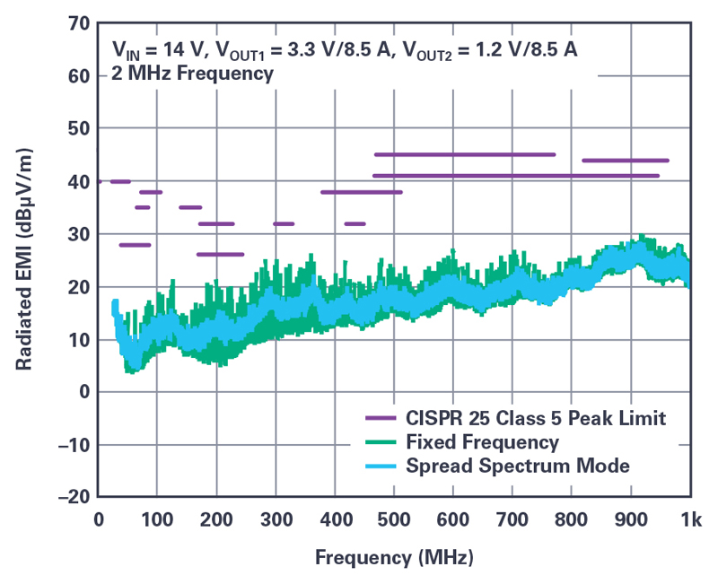
EMI/EMC compliance has become a significant concern in many electronic environments. With integrated MOSFETs, advanced process technology, and up to 3 MHz operation frequency ability, LT8652S can achieve fast, clean, low overshoot switching edges, which enable high efficiency operation at high switching frequencies, leading to a small overall solution size. With the leading-edge Silent Switcher 2 technology and integrated hot-loop caps, LT8652S can simultaneously deliver top level EMI performance and reduced switching losses. Spread spectrum operation of the switching frequency can also assist in passing EMI tests. Integrated hot-loop caps make circuits insensitive to board layout and layers. Figure 4 and Figure 5 show the CISPR22 and CISPR25 Class 5 EMI performance of the application in Figure 1.
Click image to enlarge
Figure 4. CISPR 22 radiated EMI performance for the circuit in Figure 1
Click image to enlarge
Figure 5. CISPR 25 Class 5 radiated EMI performance for the circuit in Figure 1.
Conclusion
LT8652S is an easy-to-use monolithic step-down regulator with integrated power MOSFETs and built-in compensation circuitry. It is optimized for applications with high step-down ratios, high load current, and low EMI noise requirements. A 16μA quiescent current and Burst Mode operation option make it a perfect solution for battery-powered step-down converters, significantly extending battery standby time. Its 300 kHz to 3 MHz switching frequency range make it suitable for most industrial and automotive applications. Integrated MOSFETs, along with its available 3 MHz switching frequency, minimize final solution size. CISPR 22 and CISPR 25 results show its radiated EMI performance is compliant with the most stringent EMI standards. Finally, the Silent Switcher 2 architecture of the LT8652S makes its performance impervious to layout changes and updates, simplifying the board design process.