Frederik Dostal from Analog Devices talks to PSD about bringing buck conversion to higher input voltages and the applications that this enables.
Buck converters are a great asset for power designers who wish to convert a DC signal to a lower one. They are compact, accurate, efficient, cheap and easy to design into a circuit in comparison to other options, which mainly involve using bulky transformers. One of their very few drawbacks is that there is a maximum voltage where their usefulness diminishes, which is usually at around 100V. The main reason for this is that if the input increases any higher, then the lower duty cycles cause a drop off in efficiency. Beyond that point, costs also rise, leaving and transformer-based topologies, such as fly back or forward converters as realistically the only viable option.
Frederik Dostal, Subject Matter Expert for Power Management at Analog Devices explains, “If an application needs to drop from 100V down to 3.3V, typically you’d have to select a transformer based topology, where you have a turns ratio to play with. Even in applications that don't have to be galvanically isolated, designers use transformer based topologies just to keep the duty cycle in a range that works. The rising cost is due to the need to use a higher voltage process with larger distances in-between traces for increased creepage and clearance. Silicon typically becomes larger when you have a higher voltage process, and that costs more. Additionally, even though the banner figure says 100V, in reality the useable voltage figure is likely to be a bit lower because of the need to leave an overhead. A buck converter that needs a working 100V input would likely require a headline input closer to 130V because of the overhead”.
Dostal was speaking on Analog Devices new buck converter, the LTC7897, which extends the voltage input up to 150V. The device is not a panacea for every higher voltage application, but it extends the practical voltage range of buck conversion for a limited range of applications.
These use cases include situations where the input voltage range is very wide, for example between 60V to 135V, and needs to be stepped down to around 12V at quite a high current. For example, in a 200W power supply. The duty cycle of just under 10% means a buck regulator is typically more efficient than using transformer-based technology.
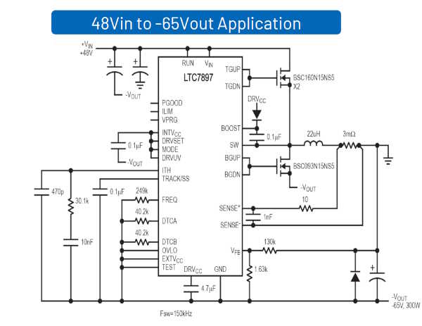
Figure 1 - the LTC7897 can generate a negative voltage when there is only a positive voltage available
A second niche application for the device is in an inverting topology, when a negative voltage is needed in a system, but there is only a positive voltage available. Figure 1 demonstrates a circuit with a 48V input and an output of -65V at a moderate current. It uses the buck regulator, but attaches the output voltage to the system ground, and then the ground of the IC becomes the negative voltage. In this case, the rating of the buck regulator has to be higher than the input voltage plus the absolute voltage of the output, 113V in total. This type of conversion has much higher efficiency than using a transformer-based topology.
The next possible application for the LTC7897 is for industrial installations that use a 72V rail, especially when there is a long power line or an inductive load. In those cases, surges can occur, and the 150V buck converter can handle those surges without using separate surge protection.
Finally, the device can be used in industrial heating systems that use the 115V rail. The heating element needs a constant current to adjust to the desired temperature. As such, the buck converter’s output voltage can be adjusted according to the temperature, very efficiently and without galvanic isolation as the LTC7897 can handle the high input voltage, and also a high output voltage.
External MOSFETs are driven using two pins - a top gate up pin and a top gate down pin. That arrangement allows the low to high switching to be adjusted differently from high to low switching, optimizing dead time and efficiency, as well as minimizing the EMI that is generated, and providing shoot-through protection. Everything can be optimized to the type of MOSFET that is selected. An LTC7897 based converter with an input voltage of 100V and an output voltage of 12V and 8A can achieve efficiency just under 96%.
The LTC7897 also has programmable gate drive voltage ranging from 5V to 10V. It supports a 100% duty cycle, spread spectrum frequency modulation, and programmable frequencies between 100kHz and 2.5MHz. The device also offers advanced protection mechanisms, including thermal, current limit, and foldback protection. In the event of a short circuit, the LTC7897 reduces the maximum sense voltage and initiates cycle skipping to limit current, ensuring system safety.

.jpg)