Best practice design recommendations
Figure 1: Supply lines - eliminate loops and decouple at local boundaries
International regulations regarding electromagnetic compatibility (EMC) affect many aspects of circuit and system design. However, there are numerous techniques that can be applied to reduce both the emissions from and susceptibility to, electromagnetic interference (EMI). Starting at the power supply end of the system, make sure that any supply line loops are minimized and the lines are decoupled at local boundaries using filters with low Q (see Figure 1). High-speed sections of the system should be placed closest to the power line input, and the slowest sections further away, to help reduce power plane transients. Make use of low pass filters on signal lines to reduce the bandwidth to the minimum necessary. On wide bandwidth lines, keep feed and return loops close. The terminations of lines carrying HF or RF signals need to be implemented correctly to minimize reflection, ringing and overshoot. Lines carrying signals external to a board are best terminated at the board edge; avoid lead terminations within the board and loose leads crossing the board. It's important that all signals on the board are tracked with no �flying leads'. To avoid resonance within a signal conductor, steer clear of cabling or tracking which is close to a quarter wavelength of the signal frequency. Slew rate limiting, that is, minimizing rise and fall times on signal and clock edges, reduces crosstalk since sharp edges produce wide HF spectra.

PCB Considerations There are quite a few things to consider when optimizing a PCB layout for EMC performance. The following aspects of board design should be avoided. The use of slit apertures, particularly in ground planes or near current paths. Also, do not use narrow tracks for power lines. This creates areas of high impedance and gives rise to high EMI. Do not overlap power planes. Keep them separate over common ground in an attempt to reduce system noise and power coupling. Track stubs should not be used. These cause reflection and harmonics (see Figure 2). Likewise, do not make localised concentrations of via and through-hole pads. Do not loop tracks, even between layers since this forms very effective receiving or radiating antenna. In the same way, do not leave any floating conductor areas - these act as EMI radiators. If possible connect to the ground plane. Often these sections are placed for thermal dissipation, hence polarity should be unimportant but check the component data sheet.

Ensure that all signal tracks are stripline and include a ground plane and power plane whenever you can. Remember that the return current from a signal line is �mirrored' in a ground plane above or below it and these mirror paths should not be interrupted or combined. Keep HF and RF tracks as short as possible and lay out the HF tracks first. Track mitring (bevelling the edges at corners) helps to reduce field concentration, which is helpful when considering EMC performance. A final tip for signal lines is to where possible, make tracking run orthogonally between adjacent layers. These tips are illustrated in Figure 2. On sensitive components and terminations, a surrounding guard ring and ground fill can be used (see Figure 3). A guard ring around trace layers reduces emission out of the board. Only connect to ground at a single point and make no other use of the guard ring (i.e. do not use it to carry ground return from a circuit).
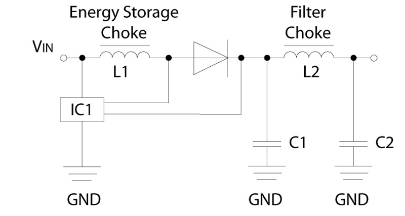
Component considerations Now, let's look at EMC considerations surrounding specific components. The first step is to locate biasing and pull up/down components close to driver or bias points. The output drive from clock circuits should be minimized. An excellent way to increase coupling between a signal line and its return and cancel stray fields between current carrying and signal lines is to use common mode chokes. Reduce component noise and power line transients by decoupling close to chip supply lines. For decoupling and bypassing, ceramic multilayer capacitors are preferred due to their low impedance, high resonant frequency and stability. Where possible, use discrete components for optimum filtering effect. Surface mount is preferable due to lower parasitics and antenna effects of terminations on through-hole parts. Include filtering of cables and over voltage protection at their terminations. This is especially important for cabling which is external to the system. If possible, all external cabling should be isolated at the equipment boundary. You can minimize capacitive loading on digital outputs by minimizing fan-out, especially on CMOS ICs since this reduces the current loading and surge per IC. Shielding, whilst effective at improving EMC performance, can be expensive and should therefore be kept as a �last resort'. Where shielding is available, use it on fast switching circuits, mains power supply components and low power circuitry. Consider specifying magnetic shields or �belly bands' around transformers or inductors and electrostatic shields between transformer windings. In general, keeping the bandwidth of all parts of the system to a minimum and isolating circuits where possible reduces susceptibility and emissions. EMC-specific components Parts like transformer isolators, standard inductors and common mode chokes can offer simple solutions to specific EMC problems within an existing circuit. Inductors Inductors are ideal for reducing EMI on power lines and for filtering high current signals. In switched mode power supply (SMPS) circuits, inductors are used for both energy storage and line filtering (see Figure 4). We recommend that a toroidal or shielded inductor be used if EMC problems are suspected. Toroidal inductors better maintain the magnetic field within the core shape and hence have virtually zero radiated field. By the same token, the susceptibility of a toroid to EMI is also very low.
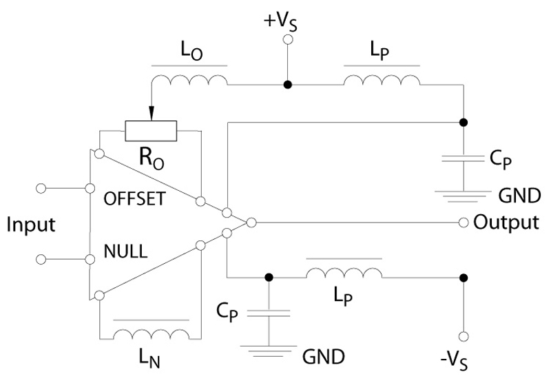
In power sections of circuits, an inductor between the local supply and the main feed provides good filtering of the supply and reduces noise from localised circuits in the system, preventing noise from polluting the main power line. To select an inductor, consider the current handling and relative switching speed of the circuit section. Generally, use the lowest value of inductance that gives the desired filtering effect as higher values have lower self-resonant frequencies which can produce troublesome ringing with circuit disturbances. A resistor across the inductor is often useful to lower the Q of the filter circuit to dampen ringing waveforms. Low inductances will also generally have lower DC losses and will produce lower transient voltages with load steps. In signal lines with a reactive load or driver, a matched termination may be required using a passive reactive circuit. The frequency response of the load/driver needs to be known, but can be matched by a relatively simple and easily characterised RCL network. Another area where inductors can be used with great benefit to the EMI of a circuit is in an amplifier bias network (see Figure 5). By using an inductive element in the bias or compensation arms, a filter can be added to the circuit without loading the signal with additional inductance. Careful choice of inductance value is required and placement close to the amplifier is essential. This method is suitable for filtering HF noise, particularly on video and TV type signals.
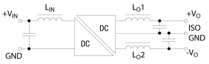
Common Mode Chokes Common mode chokes can be employed in signal lines to eliminate common mode noise or EMI on cables or induced in signal tracks. The choke should be located as near to the driver/receiver circuit as possible, or at the entry point of a signal to a board. The choke works by cancelling interference appearing on both signal and return lines (i.e. induced EMI) while allowing wanted differential mode signals and DC to pass. Choosing the right inductance will also help in maintaining a match to the characteristic line impedance and act as a filter to bandwidth-limit the termination. On power lines, common mode chokes are employed to reduce common mode EMI. Differential mode noise can also be filtered in the same component by judicious selection of a common mode choke that is deliberately designed to have less than perfect coupling between windings. This results in �leakage' inductance which acts as a series mode choke in each line. Transformers The main EMC benefit of using a signal transformer is to provide an isolation barrier between a signal line and associated circuits. This is particularly the case where the signal line exits the board or system. This is true of signals being driven or received, since isolating the line reduces common mode noise and eliminates ground (or signal return) potential differences between systems. Isolated DC-DC converters An isolated DC-DC converter can really help reduce susceptibility and conducted emissions by isolating both power rail and ground from the system supply. Isolated DC-DC converters are switching devices and as such, have a characteristic switching frequency themselves which may need some additional filtering, such as the setup shown in Figure 6. These general design recommendations should prove a useful guide to minimizing EMI and help systems achieve EMC certification first time. www.murata-ps.com


