Author:
Milind Dighrasker, Director of Application Engineering; Gautam Iyer, Senior Manager Application Engineering; and Ramesh Kankanala, Principal Engineer, all at Infineon Technologies
Date
04/20/2023
 PDF
PDF
Click image to enlarge
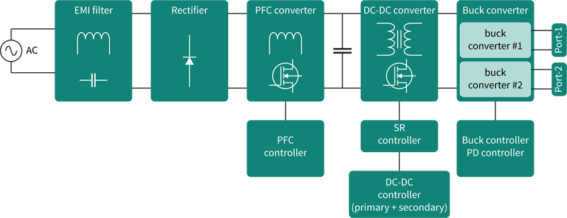
Figure 1: High-level block diagram of a multi-port adapter
Introduction
As portable electronic devices such as smartphones, tablets, and laptops have become an integral part of our lives, the need for faster charging has grown tremendously. The Power Delivery (PD) technology is designed to provide the fastest charging possible through a USB Type-C (USB-C) cable. The USB-PD Standard Power Range (SPR) standard [1] defines the maximum power that can be delivered over a USB-C cable up to 100 W. This allows for providing multiple USB-C ports (Figure 1) on universal AC-DC adapters that can charge a wide range of devices, from smartphones to gaming laptops, power tools, and even e-bikes.
However, these new requirements for higher power and multi-port have presented challenges for the converter topologies used until now. Electromagnetic compatibility, power factor correction, standby power, and average efficiency are just a few factors that need to be considered to ensure that the chargers and adapters are both effective and efficient. The size (and consequently, the power density), as well as load sharing and scaling up multiple ports, have also become more critical factors for design engineers and end-users. The power efficiency of USB-C chargers and adapters plays a crucial role in determining their power density. Hence, converter topology, usage model, integration, and flexibility of controller functionalities are all key factors to consider when selecting the right adapter architecture for your needs.
A typical block diagram of a multi-port adapter is illustrated in Figure 1. The front-end AC-DC converter is responsible for producing the requested output voltage while ensuring power factor correction (PFC) at the front end for up to 100 W of power. On the other hand, the buck converter (connected at the output of the AC-DC converter) ensures that the defined USB-C PD specifications and performance are met for multi-port adapter applications.
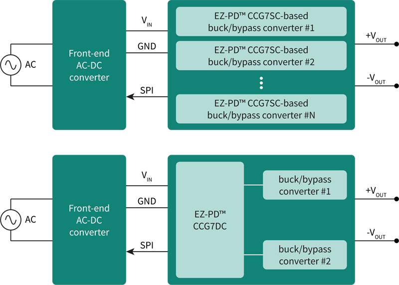
Infineon provides a comprehensive solution for both sections of adapters, i.e., AC-DC and buck converters. Specifically, for AC-DC conversion, Infineon’s EZ-PD™ PAG1 x-based solution offers a single-stage PFC design, along with the EZ-PD™ CCG7SC/CCG7DC-based buck converter, ensuring compatibility with USB PD/PPS standards. The EZ-PD™ CCG7SC is designed to support a single USB PD/PPS port, featuring an integrated buck controller and gate driver, allowing easy scaling to multi-port output. Additionally, the EZ-PD™ CCG7DC supports a dual Power Delivery (PD)/Programmable Power Supply (PPS) port, capable of controlling two buck controllers with integrated drivers, which makes it an ideal choice for dual-port or multi-port (multiples of 2) applications.
In the following sections, we will explore Infineon’s solution to the design of power adapters that meet the European standard EN61000-3-2 for power adapters. We will delve into the architecture of the conventional 100 W dual-port charger and compare it to Infineon’s new solution, examining the advantages and drawbacks of each. Additionally, we will discuss the specific features of Infineon’s EZ-PD™ CCG7SC and CCG7DC PD and buck-boost controllers, designed for multi-port consumer charging applications. Finally, we will analyze the performance of the Infineon solution and its compliance with USB-C PD with PPS specifications.
The European standard EN61000-3-2 mandates that any power adapter with a universal input delivering more than 75 W of power at a given moment requires a PFC stage. The PFC stage improves the efficiency of the power adapter by reducing the harmonic content and improving the power factor. The EN61000-3-2 standard also specifies the limits for harmonic content in four broad categories of power supplies, with explicit limits and test criteria. The objective of these limits is to ensure that the harmonic content generated by power supplies does not cause interference in other electronic devices and the power grid.
Infineon has developed a single-stage 100 W PFC design based on their EZ-PD™ PAG1x technology that meets these requirements. This design offers a significant advantage over conventional designs in terms of bill-of-materials (BOM) count and size, reducing the overall cost and making it more compact.
The architecture of a conventional 100 W dual-port charger is depicted in Figure 2. The charger follows a three-stage architecture, with the first stage being an active PFC converter, followed by a high-voltage bulk DC capacitor. The PFC converter is controlled by a Pulse Width Modulation (PWM) controller IC.
Click image to enlarge
Figure 2: Typical architecture of a 100 W dual-port charger
The second stage in the architecture is a DC-DC converter, typically a flyback controller IC, which requires a primary-side controller in addition to secondary-side feedback and compensation network. Alternatively, a secondary-side controller IC with a primary-side controller can be used.
The third stage consists of two buck converters connected to the output of the flyback converter. The buck converters are controlled by a controller IC, which also performs the PD/ PPS controller function.
However, due to the three power conversion stages, the architecture has a key disadvantage in the form of a higher bill-of-materials (BOM) count. Additionally, the DC bulk capacitor at the output of the PFC stage is typically rated for 450 V for a universal input range of 100 VAC to 265 VAC, adding to the BOM count and increasing the design’s footprint.
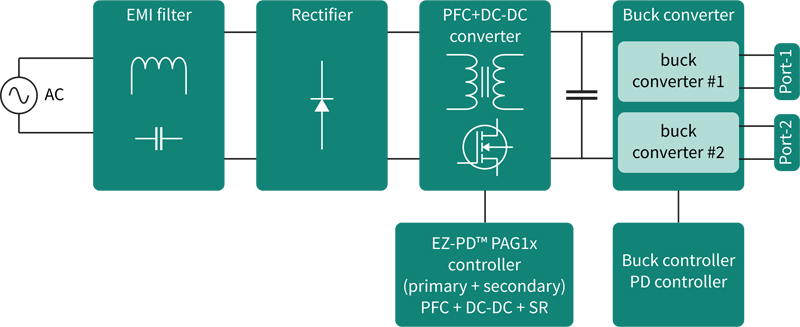
Infineon’s EZ-PD™ PAG1x enables a single-stage PFC architecture, eliminating the need for an additional PFC converter. The EZ-PD™ PAG1x is a double-chip solution with EZ-PD™ PAG1P and EZ-PD™ PAG1S and works in a secondary-side-controlled quasi-resonant (QR) flyback topology. EZ-PD™ PAG1P is a primary start-up controller for AC-DC applications and provides the start-up function, drives the primary FET, and responds to the fault condition. It is designed to work with the EZ-PD™ PAG1S in a secondary-side-controlled AC-DC flyback converter topology. In this topology, EZ-PD™ PAG1S, a single-chip, secondary-side controller that integrates the PFC controller, synchronous rectification (SR) driver, and a wide range of protection circuits, performs the voltage and current regulation. Based on these features, EZ-PD™ PAG1x offers a novel PFC, DC-DC, and SR controller functionality, addressing the key challenges of single-stage PFC designs (see Figure 3).
Click image to enlarge
Figure 3: 100 W dual-port adapter architecture with EZ-PD™ PAG1x
In this architecture, the DC bulk capacitor is located at the output of the flyback converter, which needs to be sized for 20 V of maximum PD contract voltage, i.e., it should be a 25 V-rated capacitor. Using an EZ-PD™ PAG1x-based solution has significantly lowered the BOM count, particularly for the PFC FET, PFC power inductor, power diode, PWM controller IC for PFC operation, and other passive components, including the current-sense resistor. The PFC-based flyback converter generates the required output voltage for the buck and PD controller, such as the EZ-PD™ CCG7xC, via communication lines. The PD control part is described in more detail in the following sections. Compared to the conventional design, utilizing the Infineon EZ-PD™ PAG1X-based single-stage PFC reduces the component count by nearly 80, including both active and passive components.
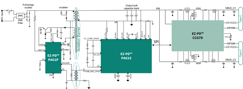
Figure 4 shows the schematic diagram for the EZ-PD™ PAG1x-based single-stage PFC with dual-port output. In this solution, the EZ-PD™ PAG1x operates with a fixed frequency of 80 kHz and functions as a secondary-side flyback and PFC controller, and SR controller. Additionally, the EZ-PD™ CCG7DC functions as a buck controller, regulating the output voltage to a lower level than the input voltage, and a PD controller, negotiating with the connected device to provide the required power and voltage levels. The communication link between EZ-PD™ PAG1S and EZ-PD™ CCG7DC ensures optimal operation and efficiency by enabling a seamless optimization of the system’s performance.
Click image to enlarge
Figure 4: Schematic diagram of EZ-PD™ PAG1x-based single-stage PFC design
Figure-5 shows Infineon’s board implementation for a 100 W PFC converter solution.
.png)
Click image to enlarge
Figure 5: Schematic diagram of EZ-PD™ PAG1x-based single-stage PFC design
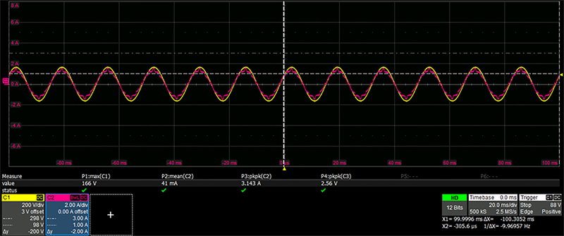
The waveform depicted in Figure 6 illustrates the input voltage and current characteristics of the 100 W PFC converter. This solution attains a power factor exceeding 0.9 for the entire input voltage range at a 100 W load while surpassing 0.98 for an input voltage of 115 VAC and a 100 W load.
Click image to enlarge
Figure 6: Channel one shows the input voltage (yellow trace), and channel two shows the input current (magenta trace)
Enhancing efficiency in multi-port charging: the role of buck and PD controllers
Infineon’s EZ-PD™ CCG7SC and CCG7DC PD and buck-boost controllers are designed specifically for multi-port consumer charging applications. These controllers comply with the latest USB-C PD with PPS specifications and come equipped with VBUS NFET and buck-boost gate drivers, as well as a high-side current-sense amplifier (HSCSA) for maximum efficiency.
The controllers allow for a maximum output voltage of 21 V from a PPS source, and fixing the front-end AC-DC converter output voltage to more than 21 V enables the use of a buck (step-down) DC-DC converter to deliver the SPR-defined voltages. However, when the required contract voltages are lower than the fixed AC-DC converter output voltage of over 21 V, there may be an efficiency penalty.
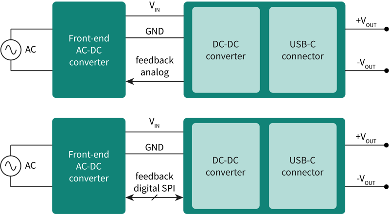
This challenge of drop in efficiency can be effectively addressed by implementing analog or digital communication between the front-end AC-DC converter controller, such as Infineon’s EZ-PD™ PAG1S, and the DC-DC converter delivering power over the USB Type-C connector. Through this communication, the controller can produce the required source voltage (ranging from 3.3 V to 21.0 V) based on the PD contract, resulting in significantly improved efficiency (Figure 7).
Click image to enlarge
Figure 7: Analog and digital communication between the buck converter and the front-end AC-DC converter
The board implementation of the EZ-PD™ CCG7SC-based buck converter is shown in Figure 8. It comprises the motherboard housing three EZ-PD™ CCG7SC controllers and buck converters for a three-port adapter solution.
.png)
Click image to enlarge
.png)
Click image to enlarge
Figures 8a & 8b: DC-DC buck and PD controller solution board
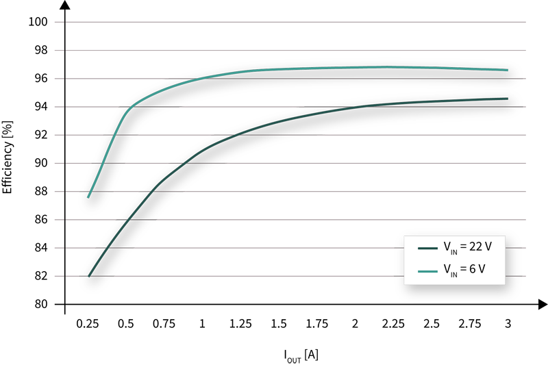
Figure 9 presents a comparison between the efficiency levels attained by a buck converter with and without the implementation of digital communication to regulate the 5 V output. The results showcase an increase in efficiency for 5 V PD contract voltage, with a potential gain of over 5 percent at light load conditions, while at full load, the efficiency gain is still remarkable, reaching up to 2 percent. The implementation of digital communication allows for a streamlined regulation of the output, resulting in improved efficiency levels that can significantly enhance the performance and overall effectiveness of the multi-port adapter.
Click image to enlarge
Figure 9: DC-DC (buck) converter efficiency comparison for 5 V output – With feedback communication between front-end AC-DC converter and DC-DC converter offering optimized efficiency (Vin = 6 V), and without feedback communication (Vin = 22 V)
In addition to the features mentioned above, EZ-PD™ CCG7SC and CCG7DC offer an innovative bypass function to achieve higher efficiency. The bypass function is designed to operate when a device connects and requests fixed output voltages (PDO), such as 5 V, 9 V, 15 V, or 20 V, complying with the USB PD standards. In this case, the front-end AC-DC converter output voltage will be directly routed to the USB-C connector via a MOSFET connected in parallel to the buck converter. By effectively bypassing the buck converter, the technique enables direct and streamlined power delivery.
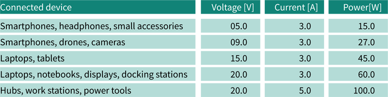
In multi-port adapter applications, flexibility is crucial in accommodating a broad spectrum of voltage- and power-rated devices (Table 1). However, predefining port voltage and power limits can significantly impede this flexibility, leading to decreased compatibility and performance. To overcome this issue, firmware-based dynamic load sharing and allocation offer an effective solution. By enabling dynamic configuration of port power, this approach ensures that all connected devices receive optimal voltage and power levels, supporting the unique power requirements of each device. By implementing this method, multi-port adapters can enhance their flexibility and overall performance, catering to a wider range of operating devices and delivering exceptional functionality.
Click image to enlarge
Table 1: Devices vs. typical power levels
The power efficiency of USB-C chargers and adapters plays a critical role in determining their power density. In addition, the converter topology, usage model, integration, and flexibility of controller functionalities are key factors to consider when selecting the right adapter architecture for your design.
In this article, Infineon demonstrated its comprehensive solution for a highly-integrated 100 W multi-port adapter with a single-stage PFC design based on their EZ-PD™ PAG1x and EZ-PD™ CCG7SC/CCG7DC technologies. The single-stage PFC architecture offers significant advantages over conventional designs in terms of bill-of-materials (BOM) count and size, reducing the overall cost and making it more compact. At the same time, it meets the European standard EN61000-3-2 for power adapters and ensures compatibility with the latest USB PD/PPS standards.
The EZ-PD™ PAG1x features a flyback secondary-side controller, a PFC controller, and a PD controller. The EZ-PD™ CCG7SC/CCG7DC offers buck and PD controller for multi-port functions. The communication between the EZ-PD™ PAG1x and EZ-PD™ CCG7SC/CCG7DC enables efficiency improvements for different PD contract voltages by adjusting the output of the flyback converter. Both ICs, are highly configurable, offering significant flexibility for custom designs for specific customer needs.
The demonstrated design offers a reliable and cost-effective solution for 100 W and 2/3 ports; however, it can be used for higher power and multi-port solutions.
Explore the capabilities of Infineon’s comprehensive solutions for highly integrated USB-C PD adapters. Visit our webpage to discover more about our highly configurable and flexible ICs, and learn how you can optimize your product with our technology.
May 9–11, 2023: Visit us at PCIM Europe in Nuremberg
You’re invited to join Infineon’s presentation of the latest trends in wide-bandgap technologies and silicon power semiconductors at our USB-C adapters and chargers demo station. Discover how our solutions address today’s challenges in green and digital transformation through our new product demos, live TechTalks on stage, or personal conversations with our experts. Meet us at Messe Nuremberg event grounds (Hall 7, Booth 412).
Infineon’s digital PCIM platform – explore now. Register and browse our highlights wherever/whenever.