Ensuring IoT Infrastructure Integrity via Smarter Nodes
With the prospect of over 17 billion IoT nodes being deployed globally in the near future, ensuring network integrity could be a huge task
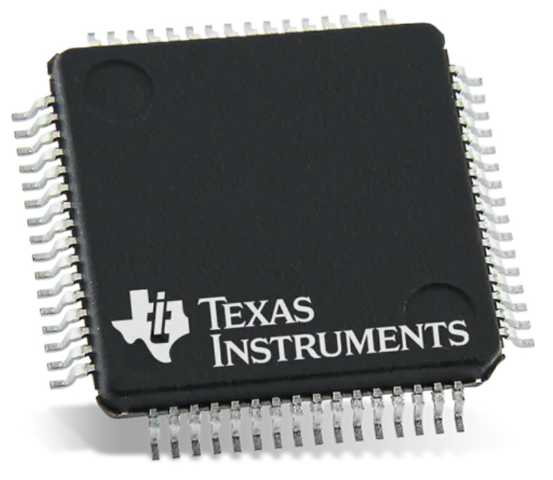
Figure 1: The Texas Instruments MSP430 MCU
IoT infrastructure can potentially be compromised in a number of ways. Firstly, there is the possibility that IoT nodes could be damaged during shipment or transport, prior to their installation. Then they might be exposed to harsh conditions, due to the application environment in which they are located - with extreme heat, high humidity or vibrational forces all posing prospective threats to long-term operation. They might also, of course, be vulnerable to physical attacks by malicious parties, or by an array of different types of security breaches.
There is an expression that a chain is only as strong as its weakest link. Now, this may not be necessarily true of all types of IoT infrastructure, especially in those that take advantage of mesh networks. However, despite having multiple nodes and self-healing capabilities, this does not mean there are adequate redundancies in place should any particular end node fail. If we consider the sheer number of IoT devices deployed worldwide, the task of ensuring on going network integrity becomes a monumental one. Recent research conducted by MarketsandMarkets suggests that the number of IoT nodes and gateways in operation will reach a total of over 17 billion units by 2023, with other analyst firms predicting it could be even higher.
With such expansive IoT networks destined to be rolled out in the near future, the constituent nodes must become smarter. They will need to be able to conduct self-checks, monitoring their circuitry for any sign of malfunction and ensuring the integrity of data collected and transmitted. Take for example an IoT node that is equipped with an accelerometer which is dropped during shipment. The accelerometer would capture the fall and impact data, then wake the MCU to perform calculations to determine the package orientation as it hit the floor (e.g., flat, on its edge or its corner). From this, it would be possible to determine whether the package had been damaged and if so transmit the information through the IoT gateway to inform the vendor or customer that a replacement will be required. When designing nodes with this capability, engineers have to consider key elements such as the MCU, memory, power management, and wireless connectivity, as well as the sensors involved. In the following article, we will focus specifically on modern MCUs that can support self-diagnostic features to help identify when a node is corrupted or damaged and then set about taking appropriate action.
The majority of IoT applications today use either 16-bit or 32-bit MCUs, depending on the complexity of the node, the available power and required data throughput. End nodes or gateway devices that need to run sophisticated algorithms will usually call for a 32-bit MCU. Encryption security (such as AES-256) is also a key requirement for modern IoT nodes.
Microchip’s PIC24E family is made up of high-performance, general purpose 16-bit MCUs with elevated code density and up to 70MIPS operation at 3.3V. These devices offer CAN communication, integrated op-amps, and motor control, USB OTG, superior ADC performance, and rapid data movement through DMA channels. They are available in small packages (down to 5mm x 5mm) with scalable memory (up to 536kB) and extended temperature ranges (reaching 150°C on certain options).
Texas Instruments' MSP430 series of ultra-low-power MCUs are available in more than 25 package configurations, featuring different sets of peripherals to address various applications. They feature a powerful 16-bit RISC CPUs, up to 512kB of flash memory and 64kB of RAM, 16-bit registers and mechanisms to maximize code efficiency. Their digitally controlled oscillators allow wake-up from low-power mode and into active mode in less than 6µs. With the backing of a broad sensing and measurement portfolio, these MCUs integrate analog and digital peripherals to reduce bill-of-material costs, ease design and improve performance. Functions encompassed include data converters, op-amps, comparators, and timers to more advanced peripherals such as capacitive touch and ultrasonic sensing. These MCUs exhibit seven low-power modes with power consumption of <100μA/MHz, 0.1μA RAM retention and <1μA RTC mode (which enables them to prolong battery life to over 20 years).
IoT-Oriented 32-bit MCUs
Analog Devices’ ADuCM3027 and ADuCM3029 ultra-low-power MCUs have 32-bit ARM Cortex-M3 processor cores that are straightforward to configure in order to get optimal performance and power consumption characteristics, while still offering the critical security and reliability functions expected in IoT deployments. These two models differ only in the capacity of the flash memory, offering 128kB and 256kB respectively (with ECC encryption incorporated in both cases). Designed for healthcare, building/factory automation, smart agriculture, and smart energy applications, these MCUs possess a 245.5 ULPBench score - based on Embedded Microprocessor Benchmark Consortium (EEMBC) evaluations. Power consumption features include active (full-on mode) at <30μA/MHz (typical), flexi (core in sleep, peripherals active) at <300μA (typical) and hibernate (with SRAM retention) at <750nA (typical). The accelerate encryption enabled by the numerous hardware and software protection mechanisms included results in strong read-protection, thus preventing any device content from being read by unauthorized users. Additionally, in-circuit write-protection precludes them from being reprogrammed with code that is not legitimate. Voltage monitoring in standby-mode and error correction for the flash memory help to ramp up reliability by avoiding corruptions that could result in operational problems or cause systems to crash.
Click image to enlarge
Figure 2: The ADuCM3027/ADuCM3029 offering from Analog Devices
NXP Semiconductors’ LPC540 32-bit MCUs combine a 180MHz ARM Cortex-M4 core with a unique power-efficient architecture, advanced HMI capabilities, and flexible communication peripherals, to deliver strong real-time performance to next-generation IoT infrastructure. Exhibiting flexibility with a quad SPI flash interface, CANbus, graphic LCD and up to 11 channels for FlexComm, they can adapt as requirements change. Compatibility within the series provides a seamless migration path for increasing processing power or adding further peripherals. Available in TFBGA180, TFBGA100, LQFP208, and LQFP100 packages, these devices feature up to 360KB of SRAM, a quad SPI Flash interface, Ethernet connectivity support, a TFT LCD controller and two CAN FD modules. They attain a compelling balance between functional integration and power efficiency, achieving an active mode current of 100µA/MHz.
Renesas’ Synergy S3A1 MCUs each come with a 48MHz 32-bit ARM Cortex-M4 CPU core, floating point unit (FPU), and a plethora of analog and security features. These MCUs have 1MB code flash memory, 8kB data flash memory and 192kB of SRAM. They are feature, pin, and IP compatible with other Synergy MCU groups, offering greater scalability and code reuse to speed up the hardware/software development process. Designed for monitoring applications (e.g., outdoor weather stations) that may require ongoing feature upgrades for multiple services, these MCUs are available in a variety of memory densities and package/pin footprints.
The members of STMicroelectronics’ STM32L4 MCU+FPU family are all ultra-low power devices based on the ARM Cortex-M4 32-bit RISC core. Operating at frequencies up to 80MHz, these cores feature a single precision format FPU, which supports all ARM single-precision data-processing instructions and data types. Full set of DSP instructions are also implemented, along with a memory protection unit that enhances application security. This family is based on a new ultra-low power platform featuring FlexPowerControl. Through its optimized power consumption levels, it achieves an EEMBC ULPBench score of 150 ULPBench-CP. The constituent MCUs offer up to 2MB of flash (dual bank) memory and up to 640kB of SRAM, as well as delivering 100DMIPS/273 CoreMark thanks to the company’s proprietary ART Accelerator at 80MHz. The entire system performance is optimized using a multi-AHB bus matrix and DMA controllers. The STM32L4 can be used to replace current designs based on the STM32F4 to get low power functionality. It has pin-to-pin compatibility, so changes to board layout are not necessary.
Click image to enlarge
Figure 3: The STM32L4 from STMicroelectronics
MCUs in Smaller Packaging Formats
Cypress Semiconductor’s PSoC 6 MCU delivers all-in-one high-performance processing and critical security features that are purpose-built for IoT applications. It is based on an ultra-low power 40nm process technology and utilizes a dual-core architecture - with an ARM Cortex‑M4 taking care of high‑performance activities, complemented by an ARM Cortex‑M0+ to execute power-constrained tasks. The active power consumption goes all the way down to 22μA/MHz for the M4 core and is just 15μA/MHz for the M0+ core. The MCU’s highly flexible architecture enables the addition of features, such as USB, Bluetooth Low Energy (BLE) and numerous other software‑defined peripherals, to create custom analogue front ends (AFEs) and digital interface circuitry that is capable of attending to IoT designs where several connectivity protocols need to be encompassed. In addition, industry-standard symmetric and asymmetric cryptographic algorithms are found on this device - including ECC and AES encryption, plus secure hash algorithms (SHA 1, 2, 3).
Microchip’s SAM R34 LoRa sub-GHz system-in-package (SIP) family includes an ultra-low power, high-performance 32-bit MCU, LoRa transceiver and software stack, which can significantly reduce time to market for IoT designs. These devices feature certified reference designs and proven interoperability with major LoRaWAN gateway and network providers. Nordic Semiconductor’s nRF52840 multi-protocol SoC is an ultra-low power, highly flexible single-chip solution suitable for short-range wireless applications. The embedded 2.4GHz transceiver supports Bluetooth 5/BLE, 802.15.4/Thread, ANT/ANT+, and proprietary 2.4GHz protocols. It is on-air compatible with the company's existing nRF52, nRF51, and nRF24 series. The dynamic multi-protocol feature of this device allows concurrent Bluetooth 5 and Thread wireless connectivity, and ensures the radio hardware’s operational time is shared between these protocols, allowing both to remain connected. This SoC is built around a 32-bit, 64MHz ARM Cortex-M4F CPU with 1MB flash memory and 256kB of RAM on chip. This CPU configuration supports DSP instructions, hardware accelerated FPU calculations, single-cycle multiply and accumulate, and hardware divide for energy-efficient processing complex operations. It employs power and resource management to maximize battery life. A voltage range spanning from 1.7V to 5.5V supports primary and secondary cell battery technologies plus direct USB supply without the use of external regulators. This device has a collection of automated and adaptive power management features, which are built into all aspects of its operation - from power supply switching to peripheral bus/EasyDMA memory management - with automated shut down of all but the absolute essential peripherals required to perform a task.
With the number of deployed IoT nodes set to ramp up dramatically in the coming years, the need to keep them all operating correctly will become increasingly acute. The MCU devices covered in this article suggest that design engineers are already starting to get access to the innovative semiconductor technology on which to execute such endeavors.
Mouser Electronics