Increasing efficiency in LED streetlight power supplies

New LLC converter simplifies design of high efficiency PSUs
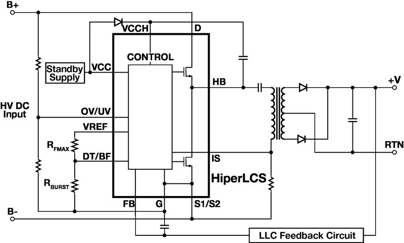
Figure 1: Shoot through due to drive-signal timing mismatch
Solid-state exterior lighting requires a regulated AC to DC power supply to drive LED loads which can vary in size from 1 W to over 500 W. To ensure a good return on investment, these power converters must offer very high efficiency—to complement the increased efficacy of the light source—and a long lifetime—due to cost and often remote or inaccessible mounting locations. The LLC converter, which runs in conjunction with a high-efficiency PFC boost conversion stage, offers the best efficiency above 100 W, but also presents some unique challenges before a reliable design can be achieved. An LLC is a resonant switching converter, which employs a half-bridge switch in series with a resonant circuit. In an LLC converter, high- and low-side drivers connect in a half-bridge configuration to a transformer via a series capacitor. The transformer's inductance and the capacitor comprise the resonant load while the two driver transistors of the half-bridge conduct alternately, leaving dead time in between each conduction phase. Variations in the drive parameters and parasitic reactances on the gates of the half-bridge MOSFETs can result in timing mismatches and possibly cause shoot through and catastrophic failure of the MOSFETs (figure 1). The risk of shoot through is the primary constraint on the switching frequency of LLC designs.
One LLC implementation makes use of the HiperLCS family of ICs from PI (Power Integrations). HiperLCS ICs integrate all the essential features and protection circuitry required for an LLC converter into a monolithic device capable of up to 440 W output (figure 2). Devices include two 530-V power MOSFETs, high- and low-side drivers, an LLC controller, UV and OV shutdown, and brown-in and -out protection.
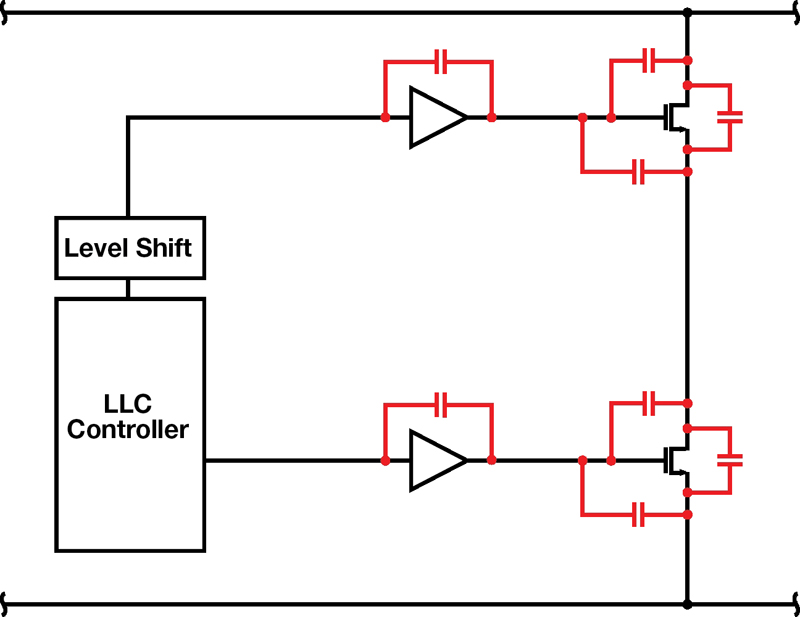
The output high-voltage MOSFETs together with the drivers, level shifter, and controller are closely coupled on a single silicon die. This enables accurate control of variations in the entire drive system, allowing compensation of all parasitic elements (figure 3). In addition, the dead time and duty cycle matching are trimmed device by device during manufacturing, with duty cycle balanced to within �1%. The accurate control of drive timing enables the IC to maintain nominal steady-state operation at a switching frequency of 500 kHz and a maximum operating frequency of 1 MHz. This high switching frequency is important because it enables the use of low-cost SMD ceramic capacitors in the output loop instead of bulky electrolytic capacitors. Ceramic capacitors are also preferred in long-lifetime applications such as area lighting, because they do not suffer from parameter drift or premature failure—unlike electrolytic capacitors which often fail at elevated temperatures. A further advantage of using a high-switching frequency is that significantly smaller transformers and output inductors are required, enabling production of low profile designs. Precise duty-cycle trimming ensures accurate duty-cycle sharing between the two output diodes and between each half of the transformer's secondary winding. Therefore it is not necessary to oversize the output diodes to accommodate current imbalances. If the duty cycle were to become imbalanced, it would be necessary to have specified the output diodes to accommodate the worst-case peak current. The transformer would also have to be designed to deliver the higher current. Clearly, efficiency would suffer because of the I2R losses resulting from the higher peak currents.
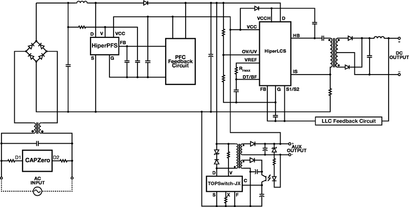
Figure 4 includes the essential elements of a complete power supply a single-chip LLC converter. At the AC supply input, a capacitor-discharge IC saves energy by preventing continuous current drain through discharge protection resistors. A high-efficiency power-factor correction front-end delivers 380 V DC to the LLC converter's output stage. A low-consumption standby-supply switcher serves two functions: first, it enables functions such as remote on-off of the main supply. Second, it delivers a 12 V DC supply to the power-factor-correction and LLC-converter ICs HiperPFS and HiperLCS devices while the main supply is in standby. Efficiency Power Integrations' HiperLCS LLC-converter ICs have two modes of use. For high-efficiency design, their resonant control circuitry provides low power loss, enabling designs that are greater than 97% efficient at a nominal 66 kHz switching frequency. If cost and size are the determining design criteria, then a high switching frequency is required. In this case, efficiency still remains high—for example, 96% at 250 kHz, the frequency where maximum power is achieved. When coupled with a power factor correcting front-end, as in figure 6, the design achieves overall efficiency levels of over 89% at full load. Modeling The HiperLCS LLC-converter ICs allow the designer to optimize a design by setting parameters such as the maximum and minimum switching frequencies and dead time to match power-train requirements. The frequency at which the supply enters burst mode is also adjustable. This allows designers to optimize the power train for maximum efficiency while still maintaining regulation at zero load during input voltage swells. With these options available to the designer, it is essential to use an accurate modeling tool to simulate the circuit's behavior and automate the design of the transformer and inductors. Power Integrations' Xls Expert Suite Version 8, a real-time design and modeling tool, supports HiperLCS designs. The software provides a complete first-pass design capability for both the transformer and resonant power train. The unique switching model within Xls is accurate to within 3%. This is a great improvement on most simplified AC models which are only accurate to 15%. The enhanced accuracy significantly shortens the design cycle by eliminating the prototyping of repeated iterations.
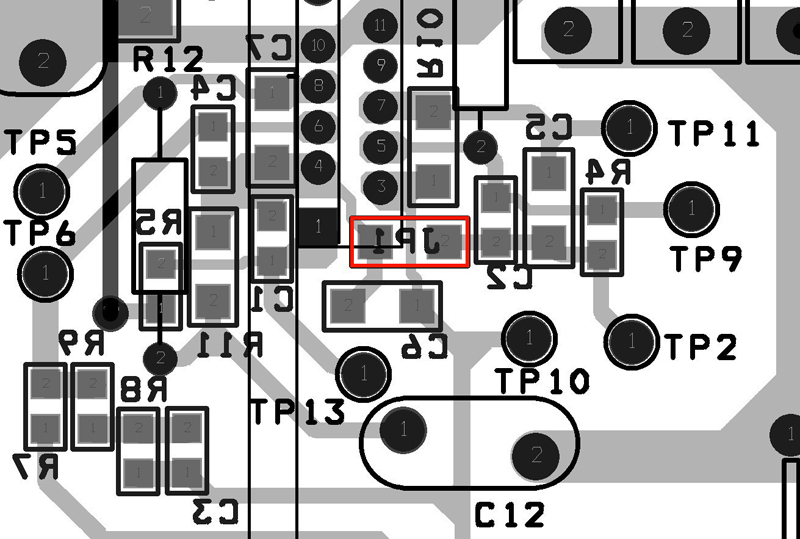
Tight layout With high currents switching at frequencies of 500 kHz, designers must understand that the placement of components and wiring traces requires careful attention in order to achieve maximum performance. Certain of the LCC-converter IC's pins of, such as the feedback pin or dead-time/burst frequency pin are sensitive to noise and therefore require decoupling. The transformer is a source of both high di/dt signals and dv/dt noise. Di/dt signals can couple magnetically to sensitive circuitry, while dv/dt signals can inject noise via electrostatic coupling. Layouts can reduce electrostatic-noise coupling by grounding the transformer core, but it is not economically feasible to reduce the stray magnetic field around the transformer without drastically reducing its efficiency. Sensitive traces and components, such as the optocoupler, should be located away from the transformer to avoid noise pick-up. Manufacturer's datasheets, application notes, and reference designs contain further detailed information of how to address component placement and trace layout issues (figure 5). For example, Power Integrations' reference design report RDR-239 describes a complete LLC-converter design appropriate for exterior lighting applications. The converter produces a 6.25-A output at 24 V with > 95% efficiency at full load. The reference design kit RDK-239 includes a working power supply, sample devices, unpopulated PCB, data sheet, comprehensive engineering report, PI Expert design software, and other related documentation. The IC deals with the matching of timing and the control of parasitics, and ready-made evaluation examples give the designer a head start. HiperLCS technology is a new resource for the roll-out of LED street and area lighting, using higher efficiency converters to provide ever greater savings in energy consumption. Power Integrations


