Increasing Ruggedness in High-Current E-FUSE Smart Switches
The speed of automotive technology innovation is accelerating as industry players develop new concepts of electric, connected, autonomous, and shared mobility
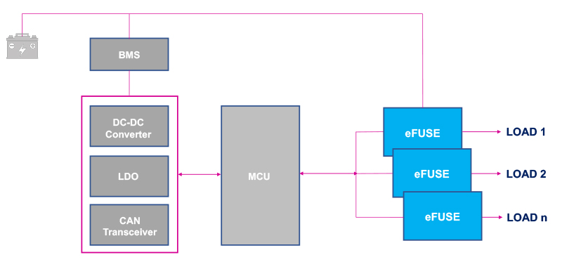
Figure 1. Block diagram of a smart automotive power distribution system
The major trend in power distribution systems is the replacement of the centralized architecture, which distributes the electric power from the battery to the individual loading systems and includes a central relay and fuse box for overload protection. The new automotive systems are based on smart power distribution with multiple small power distribution centers in a decentralized architecture. These small centers communicate each other with a local interconnect network (LIN) or controller area network (CAN). The modular implementation allows a zonal architecture in the vehicle, which strongly reduces the wire harness, thus optimizing system cost and weight in addition to the electrical performance.
The smart modules, operating as electronic fuses (eFuses), guarantee huge benefits for the enhanced diagnostic and protection associated to the real-time information exchange. In addition, the solid-state switches minimize the losses of the power distribution system, thus improving the fuel efficiency of the vehicle and decreasing CO2 emissions. Finally, eFuses increase the system reliability, fulfilling the stringent automotive safety requirements.
The block diagram of a smart automotive power distribution system is shown in Figure 1.
ST’s new STPOWER STripFET F8 40V series meets the stringent requirements for eFuse solutions in terms of high ruggedness against linear mode operation and energy management. The eFuse smart switch integrates a control circuit driven by an MCU and a power switch. For high-power automotive systems, where a high current limitation is requested, an external power switch is used, consisting of high rugged and low on-resistance power MOSFETs.
Power switch selection
The selection criteria for the external power switches are the following:
- turn ON – linear mode ruggedness for inrush current limitation;
- turn OFF – avalanche energy management.
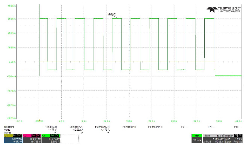
These features play a key role for the optimization of high-current power distribution systems. A comprehensive analysis is described for the eFuse smart switch in an electric power steering (EPS) system with the typical current profile, shown in Figure 2.
Click image to enlarge
Figure 2. Typical current profile of an EPS system
The maximum total current reaches 160A with a cycle time of about 40 seconds and 10 seconds of pause for a sequence of 6 times, then four power MOSFETs connected in parallel are considered with a double back-to-back configuration to ensure a bidirectional protection from battery to load and vice versa.
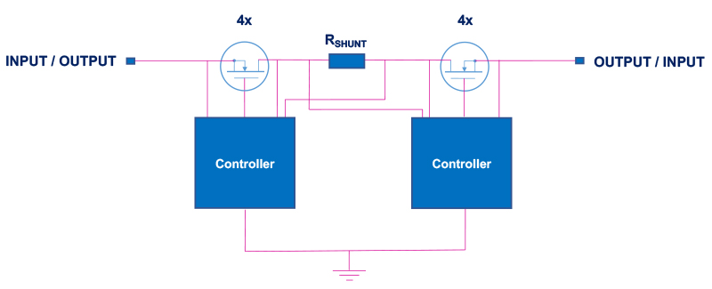
The shunt resistor (Rshunt) is inserted to detect in real time the current flowing in the branch, then turn off and shutdown the system in case of an accidental increase in current. It also helps to keep the current constant by transferring the feedback signal to the controller which tunes the gate-source voltage (VGS) of the MOSFET accordingly to limit the current to the target value.
Click image to enlarge
Figure 3. Block diagram of the eFuse system
1. Linear Mode Ruggedness
At turn on, the power distribution system has to provide a constant current for pre-charging the bulk capacitor stack of the ECU, thus limiting the inrush current and preventing any voltage spikes. This condition determines a linear mode operation for the power switch.
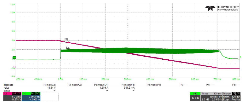
The STL325N4LF8AG was tested with a dedicated test bench at the following conditions:
VIN = 15V, C = 94mF, ID = 1.7A
and measured waveforms are reported in Figure 4:
Click image to enlarge
Figure 4. Measured waveforms for STL325N4LF8AG during the pre-charge phase
At the above conditions, the MOSFET is able to withstand the linear mode working conditions with a significant charging time of 700ms. Therefore, the safe operating area (SOA) has to be checked to verify the condition can be guaranteed as safe and reliable for the device.
The mean value of the power managed by the MOSFET can be calculated as:
P = ID x VDS_(mean) = 1.7 x (15 : 2) = 1.7 x 7.5 = 12.75 W
where: P is the power dissipated during the pre-charging phase; ID the constant drain current of the MOSFET; and VDS_(mean) is the mean value of the drain voltage of the MOSFET during the charging time.
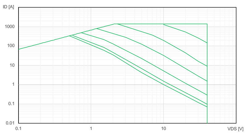
By assuming the charging time of 700ms equivalent to a steady state condition, the linear mode point on the MOSFET SOA is shown in Figure 5.
Click image to enlarge
Figure 5. SOA curves of the STL325N4LF8AG
Hence the operating point is located in a safe region of the SOA, ensuring the mandatory ruggedness level to avoid any thermal runaway. A comprehensive comparison of the SOA curves of an equivalent AEC Q101 MOSFET (same breakdown voltage and on-resistance in an equivalent package) from one of the main competitors is shown in Figure 6:
Click image to enlarge
Figure 6. Comparison of the SOA curves for STL325N4LF8AG and competing device
The STripFET F8 MOSFET exhibits wider SOA regions for pulse times starting from 1ms, showing higher margin especially at 10ms. Comparing the DC curves at 7.5V, the following values can be obtained:
- ID = 1.9A for ST’s F8 MOSFET.
- ID = 1.8A for competitor’s MOSFET.
The STripFET F8 MOSFET exhibits good steady-state performance with high ruggedness in linear mode operation perfectly aligned with the competition.
2. Avalanche Energy Management
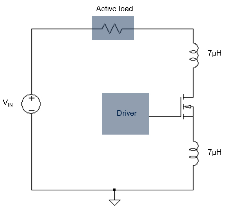
At turn off the current lasts for several µs which deposits considerable energy into the eFuse and the power switches. In fact, the wire harness that connects the main battery to the final application control board results in a high impedance associated to the parasitic stray inductance. This produces a sustained voltage spike which leads the MOSFET to the avalanche region. The eFuse failure mode at turn off is then associated to the breakdown of the drain−source junction of the MOSFET.
For the EPS system, a parasitic inductance of 7µH can roughly be considered at both drain and source connection, then the following testing circuit can be considered Figure 7:
Click image to enlarge
Figure 7. Schematic circuit for MOSFET testing at turn off
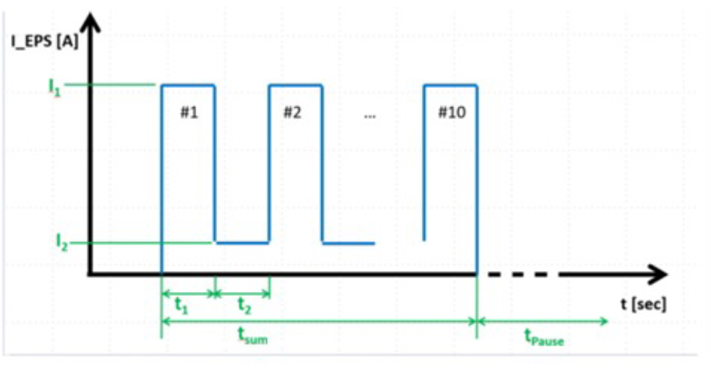
The test was performed at the following conditions related to the single power switch current profile, shown in Figure 8:
I1 = 40A, I2 = 4A, t1 = 2.1s, t2 = 2s
Click image to enlarge
Figure 8. Current profile of the single power switch
The STL325N4LF8AG can withstand the loading current for 39s, reaching a stable value of the maximum case temperature (Tc ) of 60.7°C at the end of the test.
At turn off, the MOSFET enters the avalanche mode, by reaching a maximum value of the drain-source voltage of 47.2V which exceeds the breakdown voltage. In this condition, the device has to manage a single pulse avalanche energy (EAS) of 16.8mJ for an avalanche time (tAV) of 20µs
The avalanche condition is reliable and safe for the MOSFET if the operating temperature remains lower than the absolute maximum rating value (equal to 175⁰C). In this case, the EAS energy for tAV = 20µs determines a power dissipation (PD) of 840 W
From the datasheet, the thermal impedance value relevant to tAV = 20µs is the following
Zth = K (@ 20µs) x RthJC = 0.023 x 0.8 = 0.018 ⁰C/W
Then, the temperature variation (DT) is given by:
DT = PD x Zth = 15 ⁰C
and, with an initial junction temperature (TJ_in) of 25⁰C, the operating temperature (TJ_oper) in avalanche condition becomes:
TJ_oper = TJ_in + DT = 25 + 15 = 40 ⁰C
This ensures the STL325N4LF8AG device can safely manage the discharge energy in the eFuse system.
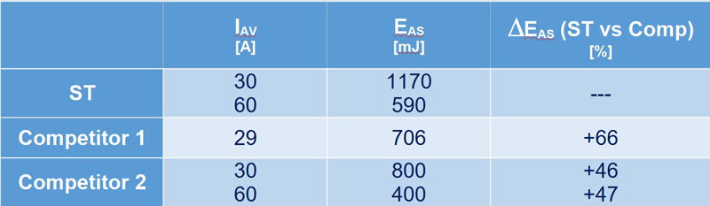
A comprehensive comparison of the guaranteed EAS values of an equivalent AEC Q101 MOSFETs from the main competitors is reported in Table 1:
Click image to enlarge
Table 1. Comparison of EAS at different avalanche current values for ST and main competitor devices
Then, the innovation introduced with new trench structures to ST’s STripFET F8 technology deeply increases the performance not only in switching, but also in avalanche conditions, making the MOSFET operate in safe and reliable mode.


