Industry-leading class D amplifiers at every power level: Part 1 of 4 Editorial Series sponsored by Infineon; “Class D Amplifier Solutions For Audio Applications at Every Power Level”
How continuous innovation enables Infineon to offer products and application solutions at every power level
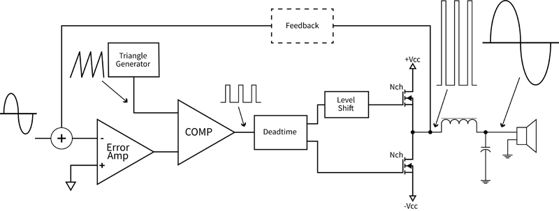
Figure 1. Block diagram of a class D audio amplifier
Making yourself heard can be challenging in a world where everyone seems to have something to say. However, one way to gain an advantage is by choosing a sound system that delivers unsurpassed audio quality using a high-efficiency class D amplifier.
In this four-part series of articles, Infineon discusses speaker design requirements for various audio applications, including low-power consumer portable equipment (<50 Watts), mid-power domestic, commercial, and professional applications (50 to 250 Watts), and finally, at significantly higher power levels like those required in industrial environments and entertainment venues like concert theatres and stadiums (250-5000 Watts).
Each article presents a class D amplifier solution for applications at a different audio power level before the series concludes with Infineon sharing its vision for the future of class D audio. This first article revisits the theory and operation of the class D amplifier to explain its advantages to audio applications compared to other amplifier classes and design pitfalls that can result in poor audio performance.
Understanding audio amplifier classes
Audio amplifiers are divided into different topologies, or classes, reflecting the percentage of the input signal cycle for which output driver devices conduct.
In a Class A amplifier, a single output driver conducts for the entire duration of the input signal cycle. While this topology is the most linear, it is also the least efficient since only 20 percent of the available power typically appears at the output. Class B amplifiers use two complementary output drivers, which conduct on one-half of the input signal cycle respectively. If no input signal is present, no current flows, and while this raises amplifier efficiency to about 50 percent, the linearity of this topology is not as good as class A because distortion is introduced at the crossover point as a result of the delay turning one output driver off and the other on.
Class AB amplifiers combine the functionality of classes A and B. In this topology, both drivers conduct simultaneously for a short duration close to the crossover point. This means each conducts for more than half but not the entire input signal cycle. Consequently, they can almost match the linearity performance of class A while achieving the efficiency of class B, but this is typically only about 50 percent.
Class D amplifiers are designed NOT to be linear
In contrast to the linear amplifier classes previously discussed, the class D amplifier topology typically uses MOSFET switches that are switched either entirely on or fully off using a pulse-width modulated (PWM) signal. This significantly reduces power losses enabling efficiencies of 90-95 percent. First, the audio signal modulates a PWM carrier, which then switches the output drivers – these are then followed by a low pass filter to remove the high-frequency signal components.
The basic block diagram for a half-bridge class D amplifier, with the waveforms at each stage, is shown in Figure 1. This circuit uses feedback from the half-bridge output to help compensate for variations in the bus voltages.
Class D amplifier operation
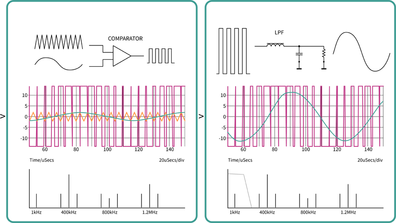
The operation of a class D amplifier is similar to that of a PWM power supply but has an audio sinusoidal signal input with a frequency ranging from 20 Hz to 20 kHz (the range of audible frequencies for humans).
First, this signal is compared to a high-frequency triangle or sawtooth waveform to generate the PWM signal shown in Figure 2 below. Next, this PWM signal drives the power stage to create the amplified digital signal. Finally, the output signal is low pass filtered to remove the PWM carrier frequency and retrieve the sinusoidal audio signal.
Click image to enlarge
Figure 2. Waveforms at each stage of a class D amplifier
Class D amplifier topologies
Like linear amplifiers, Class D amplifiers can be further categorized into sub-topologies – half-bridge and full-bridge.
While each has relative advantages and disadvantages, the full bridge offers better audio performance for several reasons. Effectively combining two half-bridges, it has more components and is, therefore, bigger, but its differential output structure inherently cancels even-order harmonic distortion components and DC offsets. A full-bridge topology also allows a three-level PWM modulation scheme, with fewer quantization errors, to be used. Later we will introduce the MERUS™ solution from Infineon, which features industry-leading five-level PWM.
Differences between linear and class D amplifiers
Whereas linear amplifiers have constant gain irrespective of variations in bus voltages, for class D amplifiers, the gain is proportional to the bus voltage. This means that while linear amplifiers’ power supply rejection ratio is typically excellent, the PSRR of a class D amplifier is 0 dB (i.e., it cannot reject any variations in the power supply voltage), so feedback compensation is commonly used.
In linear amplifiers, energy flow is always from supply to load, and this is also the case in a full-bridge class D amplifier. However, in half-bridge and full-bridge class D topologies, energy flow is bi-directional, and excess energy stored in the output LPF results in a phenomenon called “bus-pumping.” This is mainly noticeable at low audio frequencies (below 100 Hz) but also occurs across the entire audio band. However, at higher frequencies, pumping is absorbed by the bus capacitor, so voltage fluctuations are not as noticeable.
Factors that can negatively impact class D amplifier performance
An ideal class D amplifier should be 100 percent efficient with no distortion and no noise in the audio band. However, practical amplifiers have imperfections that cause distortions and noise. These are mainly due to the distorted switching waveform generated in the class D stage as a result of:
› Non-linearity in the PWM signal from the modulator to the switching stage due to limited resolution and jitter,
› Timing errors added by the gate drivers, such as dead-time, ton/toff, and tr/tf,
› Unwanted characteristics in the switching devices, such as finite resistance (RON) and switching speeds or body diode characteristics,
› Parasitic components which introduce ringing on transient edges,
› Power supply voltage fluctuations due to finite output impedance and reactive power flowing through the DC bus,
› Non-linearity in the output LPF.
In general, timing errors in the gate-switching signal are the primary cause of non-linearity, with dead time making the most significant contribution. A small amount of dead time in the tens of nano-seconds can quickly generate more than 1 percent of total harmonic distortion (THD), meaning accurate switch timing is always a primary concern in class D audio amplifiers.
Like other switching applications, electromagnetic interference (EMI) is also troublesome in class D amplifier design. One of the significant sources of EMI is the reverse recovery charge of the switching MOSFET body diode flowing from the positive power rail to the ground. During the dead time (deliberately inserted to prevent shoot-through current), the inductor current in the output LPF causes the body diode to turn on. In the next switching phase, when the other side of the MOSFET begins to conduct (at the end of the dead time), the body diode stays in a conducting state unless the stored minority carrier is fully discharged.
This reverse recovery current typically has to have a profile with sharp edges, leading to unwanted ringing from stray inductances in the printed circuit board (PCB) traces and on packaging pins. Therefore, careful PCB layout is crucial for both design ruggedness and reducing EMI. It is also important to note that designing a class D amplifier with a narrow dead time can be risky in mass-produced devices where it can vary from unit to unit and with die temperature. Significant mismatches could cause both high and low-side MOSFETs to be turned on simultaneously, meaning the DC bus voltage is short-circuited by the MOSFETs, potentially leading to device destruction. For a reliable class D amplifier design, it is vital to ensure that the dead time is always positive (and never negative) to prevent MOSFETs from entering the shoot-through condition.
Conclusion
This article provided an overview of how class D amplifiers operate and their advantages over linear amplifier classes in audio applications. It also discussed some pitfalls that can lead to poor class D amplifier designs.
Armed with this knowledge, the second article of this 4-part series discusses design requirements for using low-power audio applications and how Infineon has developed tailored class D solutions to address these. Watch out for it.
For more information, please visit our MERUS™ class D audio amplifier IC website. Click here.


