It's Time to Rethink Power Semiconductor Packaging
When the issue invariably turns to the packaging of the power semiconductor the requests for improvement fall into six categories....
In my 40 years’ experience in power semiconductors, I have visited thousands of customers, big and small, on every continent except Antarctica. When the issue invariably turns to the packaging of the power semiconductor – transistor, diode, or integrated circuit – the requests for improvement fall into six categories:
1. Can you make the package smaller?
2. Can you reduce the package inductance?
3. Can you make the product with lower conduction losses?
4. Can you make the package more thermally efficient?
5. Can you sell the product at a lower price?
6. Can you make the package more reliable?
When people think of wide bandgap power semiconductors, they are usually thinking of gallium nitride (GaN) or silicon carbide (SiC). This article will focus on lower voltage GaN-on-Si power device packaging because that is where designers of power systems are most pressed to reduce system size, cost, while increasing efficiency and power density.
So, why do we even need a package? In fact, semiconductor packages only degrade the performance of a power device by adding thermal and electrical resistance, inductance, size, cost, and reliability problems. The key reason packaging is required is to protect silicon devices from the environment – humidity in particular.
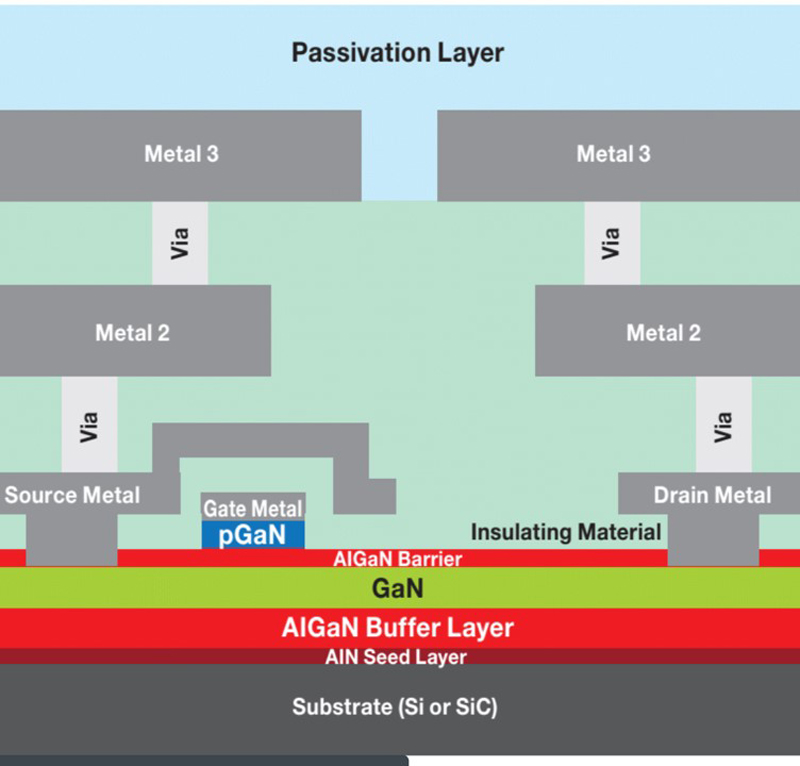
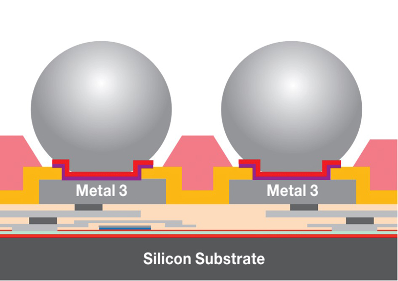
GaN-on-silicon has some amazing advantages over silicon power MOSFETs. In addition to much, much superior device performance, the thin layer of GaN in which the active devices are manufactured can be sealed under multiple layers of glass during the standard fabrication process. These layers of glass effectively protect the device from the environment, something silicon MOSFETs cannot do easily because the entire silicon-on-silicon structure is electrically active. The lateral GaN devices are only active on the surface attached to the PCB (See Figures 1 and 2).
1a
1b
Click image to enlarge
Figure 1 (a) cross section of a GaN-on-Si transistor with the top passivation layer, and (b) the same structure with solder bumps formed. Note that the glass seal completely protects the underlying device from humidity
Click image to enlarge
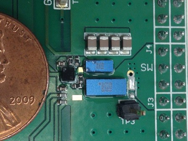
Figure 2: Two EPC eGaN FETs are soldered to a PCB with the active area facing down. The blue back surface is silicon nitride on top of silicon
GaN transistors are much smaller than their silicon counterparts. This size advantage translates into additional cost benefits to the GaN device maker, and it translates into additional cost benefits to the user. PCB real estate is very expensive. Smaller devices mean less real estate.
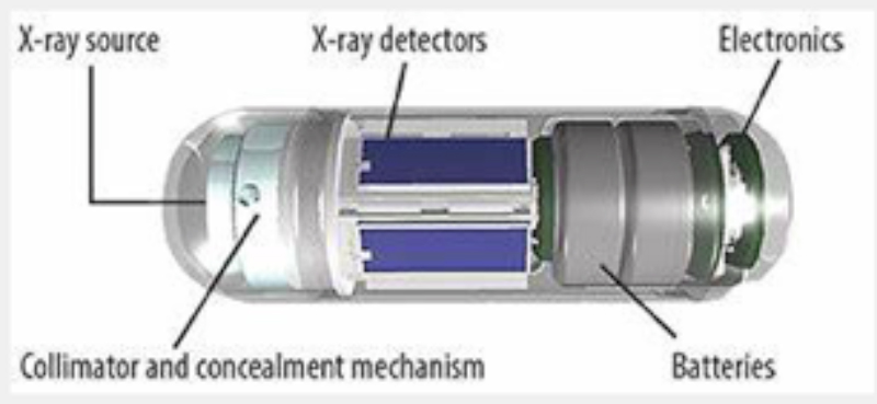
In some cases, the smaller footprint and greater performance of GaN enables a new end product not possible with larger silicon parts. Figure 3 is an example of the power of “small size.” In this figure is a miniaturized X-ray machine in a pill that you swallow. The result: the X-ray pill performs a colonoscopy without prior purging. The high-resolution images of the colon are wirelessly transmitted to a receiver worn as a patch on the patient’s back. The cost of the pill is low enough that it does not have to be recovered after use (Whew!). Can’t do it with silicon; just can’t!
Click image to enlarge
Figure 3: This X-ray pill from Check Cap can do a full colonoscopy without prior purging. A high resolution image of the colon is beamed wirelessly to a receiver worn as a patch on the patient’s back
Small has other advantages. Small devices can be located closer to other devices in a circuit. This reduces unwanted inductance and can reduce the overall size of the circuit design. Stray, or parasitic Inductance, is the enemy of a power system in that it causes the circuit to react more slowly and “ring” with voltage and current oscillations. This ringing can damage devices in the circuit and cause unwanted noise that may need to be filtered out.
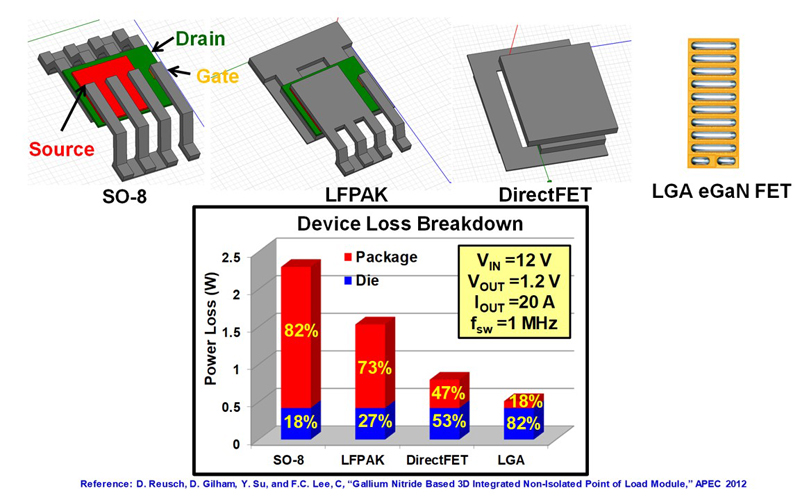
Figure 4 shows the impact of just the inductance inside silicon MOSFET packages on the power losses in a common power supply. In this case, the internal package inductance causes the devices to turn on and off slower and therefore the transistor generates higher switching losses. The popular SO-8 package induces losses that amount to 80% of the total losses incurred in the device. Even the most efficient package – the DirectFET, a clever heat dissipating package – doubles the losses in the device. The EPC2001C chip-scale device has less than 20% losses added due to inductance in the traces on the PCB under the device. Lower losses, less heat, higher power conversion efficiency. In addition, the chip-scale package doesn’t add any unwanted resistance to the device. Package resistance can add 20-50% to the resistance of a low voltage state-of-the-art silicon MOSFET. This added resistance contributes to additional power losses, or additional costs when compensated for the added package resistance by increasing the size of the silicon chip.
Click image to enlarge
Figure 4: Popular power packages such as the SO-8, LFPAK, and DirectFET add considerable parasitic inductance to a power conversion circuit. This inductance induces large losses in the transistor inside the package
When customers see the tiny eGaN transistors or ICs many of them worry about their ability to remove the heat from the part. Power losses in the transistor generate heat. Thus, this heat must be removed or the device, and the entire system, may overheat. The best way to get rid of heat is not to generate it in the first place. In the above paragraphs we explained that GaN-on-silicon devices are much more efficient than silicon-based devices and therefore generate less power losses and less heat.
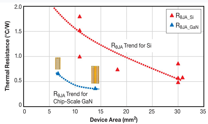
However, an amazing attribute of a package-less device is that it is much more thermally efficient than a MOSFET in the best power package. Figure 5 is a comparison between eGaN FETs and DirectFETs. In the figure, the vertical axis is the thermal resistance from the device to the ambient and the horizontal axis is the device size. The lower the resistance the better, and eGaN FETs in chip-scale “packages” are much better. It is not a surprise, because eliminating all barriers between the active device and the ambient environment gives heat the most direct path to the outside world.
Click image to enlarge
Figure 5: Chip-scale packages have lower thermal resistance than the most efficient silicon packages
Size, inductance, conduction losses, thermal resistance, and cost – chip scale beats packages every time!
What about reliability?
Experienced users and producers of power semiconductors will all tell you that it is the package that causes the most reliability problems. Packaging induces high stress on the silicon device during the encapsulation processes. Multiple dissimilar materials are used in a package to create a protected and sealed environment, but these dissimilar materials tend to grind against each other and come apart during thermo-mechanical stress.
Over nine years and 30 billion device hours in actual operation, eGaN FETs and ICs from EPC have demonstrated an unprecedented record of reliability in the field. Whether it be in truck headlamps, on board autonomous vehicles, inside 4G/LTE base stations, or within DC-DC power supplies, eGaN devices have demonstrated a total field failure rate of under 1 FIT (failures every billion device hours).
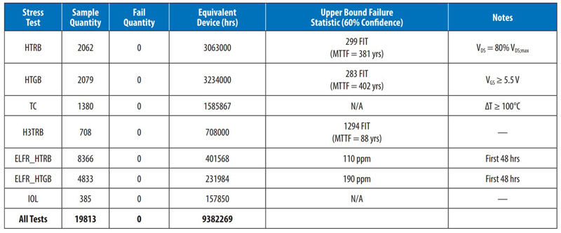
In addition to achieving AEC Q101 qualification in 2018, eGaN FETs and ICs have undergone more than 9.3 million hours of in-house stress testing without a single failure. Table 1 lists the types of tests and the conditions that eGaN devices have completed. Note that even under high humidity testing, eGaN devices in chip-scale packages can withstand as much (or more) than any traditional plastic package.
Click image to enlarge
Table 1: Summary of stress test data for eGaN Devices
The six key attributes of a better package; size, inductance, resistance, thermal efficiency, cost, and reliability all point to the future of packaging for GaN FETs and ICs as being – package-less -- that is, no package at all!
EPC – Efficient Power Conversion


