PoE++ allows 1.7 A at 52 V to be sent over the same cabling with Gigabit Ethernet, laying the groundwork for the next-generation of power-hungry applications
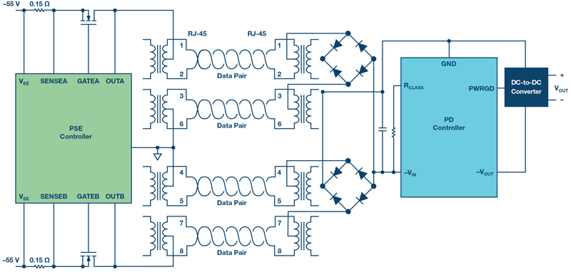
Figure 1. Power over Ethernet block diagram.
Five years in development and set to finalize in late 2018, IEEE’s next Power over Ethernet (PoE) standard, also known as PoE++, has power sourcing equipment (PSE) and powered device (PD) developers scrambling for the latest hardware, and rightfully so as PoE++ delivers up to 71.3W to the PD, nearly tripling the previous standard’s 25.5 W. PoE++ allows 1.7 A at 52 V to be sent over the same cabling with Gigabit Ethernet, laying the groundwork for the next-generation of power hungry applications—think outdoor heated pan-tilt-zoom camera networks or long-range base stations and access points for cellular or Wi-Fi communication.
Figure 1 shows a basic PoE block diagram, with a single PD connected to a PSE. Now that the 802.3bt standard has finalized, PoE developers will want to be first to market with their PoE++ designs. The challenge becomes finding fully released and qualified PSE and PD solutions 100% compliant to the 802.3bt standard. Look no further …
As PoE pioneers and active members of the IEEE 802.3bt Task Force, Analog Devices has released PoE++ PD and PSE controllers that enable PoE developers to design to the final version of the 802.3bt standard. The release of the Analog Device LTC4291-1/LTC4292 PoE++ PSE controller chipset and PoE++ PD controllers enables developers to offer a complete end-to-end PoE++ system that is both tried and proven in the field. We’ll take a closer look at what makes the LTC4291-1/LTC4292 chipset special and describe how it augments the IEEE’s latest PoE standard, as well as quickly revisiting the key features of the PoE++ PDs products.
The LTC4291-1/LTC4292 PSE Chipset
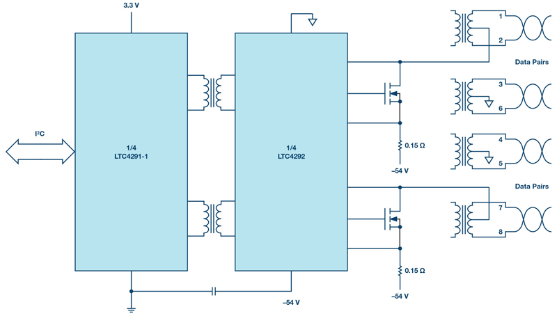
The LTC4291-1/LTC4292 is an isolated 4-port PSE controller chipset specifically designed for PoE++ systems. Figure 2 is a simplified schematic of the LTC4291-1/LTC4292 that shows how one of four Ethernet ports is powered. The most novel feature of the chipset is its integrated isolation, hence the chipset architecture, where the LTC4291-1 provides an isolated digital interface to the PSE host, while the LTC4292 provides a high voltage Ethernet interface. IEEE 802.3 Ethernet specifications require that network segments, including PoE circuitry, be electrically isolated from the chassis ground and the PHY. By placing the LTC4291-1 on the non-isolated side and the LTC4292 on the isolated side, up to six expensive optocouplers and an isolated supply are replaced with a cheaper, more reliable, 10/100 Ethernet transformer. This topology results not only in cost savings, but also in a more robust and manufacturable PSE design.
Click image to enlarge
Figure 2. Simplified schematic of LTC4291-1 and LTC4292 PoE++ quad PSE chipset.
Users can communicate with the LTC4291-1/LTC4292 through the I2C interface and can select one of four PSE operating modes (auto, semi-auto, manual, or shutdown), depending on the application. The LTC4291-1/LTC4292 uses two channels (two gate drivers) to control the power path via external MOSFETs as low as 40mΩRDS (on). The use of external MOSFETs allows users to select low RDS(on) components, reduce power dissipation, and decouple channel failures. The use of 0.15Ω sense-resistors also reduces power dissipation. The I2C interface allows port configuration, port status monitoring, and telemetry readings of port current, PoE supply voltage, and port power.
802.3bt introduces two different PD signature configurations, single- and dual-signature PDs. A single-signature PD (Figure 3) is a PoE++ PD that shares the same detection signature and classification signature between both pairsets. A dual-signature PD is a PoE++ PD with an independent signature on each pairset; allowing each pair set to have fully independent classification and power allocations. Dual-signature PDs are complex solutions costing twice as much as a single-signature PD. Further, it is worth noting that 802.3bt dual-signature PDs are not equivalent to pre-standard UPoE devices, despite sharing a common architecture. The LTC4291-1/LTC4292 supports an updated PoE++ PD detection process incorporating the new connection check sub-procedure to determine which PD signature configuration is attached to the PSE.
Click image to enlarge
Figure 3. Single-signature vs. dual-signature PD topologies.
Once a connection check is performed, the LTC4291-1/LTC4292 proceeds to verify the connected PD is IEEE-compliant. While IEEE requires PSEs to detect valid PD signatures (25 kΩ) using either a 2-point voltage or 2-point current detection scheme,the LTC4291-1/LTC4292 implements a more robust scheme by employing both types of detection schemes. This multi-point (multiple voltages and multiple currents) detection scheme is used to eliminate false positives and avoid damaging network devices that were not designed to tolerate PoE dc voltages.
PoE++ energizes four pairs of conductors (eight wires) to deliver power as compared to the traditional two pairs of conductors (four wires) used by previous PoE standards. Not only are the new, higher power levels enabled, but the use of more conductors provides better efficiency for the older, lower power levels since the power loss in the cable is cut in half.
Take, for example, a PoE+ PSE required to supply 30W to ensure a PoE+ PD will receive 25.5 W, where 4.5 W is lost over 100 m of CAT5E cable. Powering the same 25.5 W PD with the PoE++ standard would typically reduce the loss to less than 2.25W, increasing the overall power delivery efficiency from 85% to 92.5%. When you consider the number of PoE PDs in the world, this translates to a very large reduction in power and, in many cases, up to a 7.5% lower carbon footprint.
We have four new PoE++ non-isolated high-power PD classes, bringing the total number of single-signature classes to nine as shown in Table 1. Classes 5 through 8 are new to PoE++ and translate to PD power levels ranging from 40 W to 71.3 W. PSEs still have their choice of using the physical layer (that is, 5-event classification for 71.3W) or data link layer (for example, link layer discovery protocol (LLDP)) to classify PDs, and PDs still need to be able to support both classification schemes to be compliant. Remember that, because each pair set operates independently in a dual-signature PD, each pair set can be a different class. For example, a Class1 (3.84W) on the first pair set and a Class2 (6.49W) on the second pair set would make for a dual signature Class 1, Class 2 (10.3 W) PD.
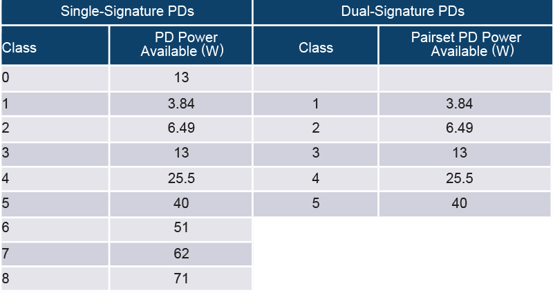
Click image to enlarge
Table 1. PoE++ PD Classes and Power Levels
PoE++ PDs may also implement an optional extension of physical layer classification, known as Autoclass, where a PoE++ PSE, like the LTC4291-1/LTC4292, measures the actual maximum power draw of a connected PD. By doing so, this handy power management feature allows, for example, the LTC4291-1/LTC4292 to allocate leftover power to their light bulbs if it measures a particular bulb, due to lower brightness settings or a shorter cable, drawing less than its classpower.
It goes without saying that PoE++ is backward compatible with the older 25.5W PoE+ and 13W PoE standards. A lower-power PoE+ or PoE PD can connect to a higher power PoE++ PSE, like the LTC4291-1/LTC4292, without any issues. And, when the tables are turned and a higher power PoE++ PD is connected to a lower power PoE+ or PoE PSE, the PD can operate in the negotiated lower power state—this is referred to as demotion. If a PD ignores demotion and operates at its highest power state, the power-hungry PD will cause the PSE to repeatedly turn on, hit its overcurrent, then turn off—in effect, motor boating the PSE. For this reason, demotion is required by both PoE+ and PoE++, but is unfortunately overlooked in some implementations.
PD Implementations
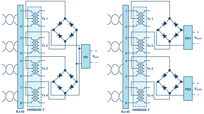
Developers use Analog Devices ICs to maximize PoE++ PD performance. Figure 4 shows a simplified block diagram of a high efficiency, single-signature PoE++ PD interface with an auxiliary input. This solution provides an end-to-end (RJ-45 input to PD load) efficiency of greater than 94% and operates within the –40°C to +125°C temperature range.

Click image to enlarge
Figure 4. Simplified block diagram of a high efficiency IEEE 802.3bt single-signature PD interface with auxiliary input.
The LT4321, shown at the RJ-45 interface in Figure 4, is an active diode bridge controller that replaces the required diode bridge rectifiers. The LT4321 uses low loss N-channel MOSFET bridges to simultaneously increase the PD’s available power and reduce heat dissipation. PoE++ requires PDs to accept dc supply voltages of any polarity over their Ethernet inputs, so the LT4321 smoothly rectifies and combines power from both data pairs into a single, polarity correct supply output. Overall circuitsizeandcostarereducedastheenhancedpowerefficiencypractically eliminates heat sinking requirements, and power savings of 10× or more enable PDs to stay within classification power budgets or add additionalfunctionality.
Following the ideal diode bridge controller in Figure 4 is the brains of the PD interface—the LT4295 is a PoE++ PD interface controller that integrates a high efficiency forward or no-opto flyback controller. The LT4295 supports all nine IEEE PD classes with an integrated 25 kΩ signature resistor, up to 5 event classification, and a single-signature topology. Aside from providing more PD power, what gives the LT4295 an edge over traditional PD controllers is its use of an external power MOSFET to, again, drastically reduce overall PD heat dissipation and maximize power efficiency, which becomes more important at PoE++ standard’s higher power levels.
For those PoE++ PD designs that need to be able to support an auxiliary supply, where the PD can be optionally powered by a power adapter, the LT4320, shown at the top of Figure 4, is a 9 V to 72 V active diode bridge controller that replaces each of the four diodes in a full-wave bridge rectifier with a low loss N-channel MOSFET to significantly reduce the power dissipation and increase available voltage. Power supply and wall wart sizes can be reduced as the enhanced power efficiency eliminates bulky and costly heat sinks. Low voltage applications can also benefit from the extramarginaffordedbysavingalmosttwofulldiodedrops(~1.2V,which is 10% at 12 V) inherent in hot-running diode bridges, increasing the application headroom.
Conclusion
The PoE++ standard’s ratification is imminent, so developers can confidently go to market. PoE++ standard's higher power levels up to 71.3W are supported with a wealth of new power management features that developers can take advantage of to create more dynamic and optimized systems. PSE developers should appreciate the robustness and BOM simplification of Analog Devices’ just-released LTC4291-1/LTC4292 PSE quad-port chipset. Meanwhile, at the other end of the cable, PD developers continue to have multiple Analog Devices ICs at their disposal to reduce heat and increase power efficiency.
Analog Devices