Author:
Tiziano Pastore, Sr. Director – Applications Engineering, NexGen Power Systems
Date
05/31/2022
 PDF
PDF
Click image to enlarge
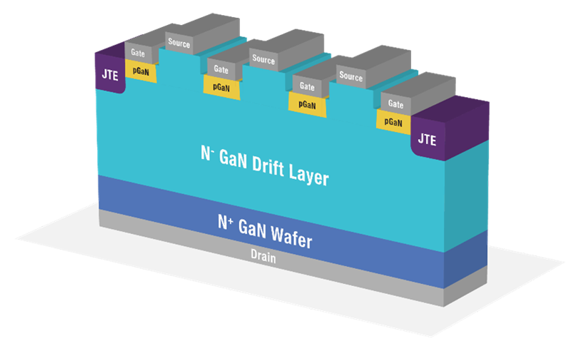
Figure 1: NexGen Vertical GaN. The GaN Drift Layer grows on a GaN wafer
The lighting industry continues to push innovation in LED applications. First, more compact designs are needed without sacrificing light quality. As designs become sleeker, light sources can disappear into the background and consumers can enjoy their lighting without having to see the direct light source, or worse, the power electronics energizing it, mimicking the feel of a naturally lit indoor space. In addition to becoming sleeker, these lighting systems also need to be smarter and more “communicative”. Human centric lighting demands designs that automatically adapt to users' preferences and behaviors.
In addition, lighting designs are requiring higher power and higher overall performance in order to serve newly emerging use cases, such as horticulture. Higher efficiency lighting systems are needed as well to keep up with industry demands. However, design limitations exist using traditional silicon-based solutions. NexGen Vertical GaN power device technology unlocks the potential of GaN for the lighting industry enabling smaller, more efficient designs that will drive the high performance, sleek and smart LED designs for years to come.
Vertical GaN
Vertical GaN provides power devices with extremely low output capacitance, allowing switching frequencies in excess of 1 MHz while maintaining high efficiency. The power device used in the application has a breakdown voltage of 700 V, with a typical RDS(ON) of 1 Ω at 25°C and a COSS of 3.6 pF at VDS = 400 V. NexGen Vertical GaN devices are made of Gallium Nitride (GaN) grown vertically on a GaN wafer (see Figure 1). This construction decouples the breakdown voltage from the device area, creating high voltage, avalanche-rated devices carrying large current densities while still operating at very high frequencies.
In order to maximize the benefits of this game-changing technology, NexGen Power Systems pairs its Vertical GaN JFET with a flexible controller that provides closed loop regulation and high frequency sensing, together with scalability to multiple power levels and topologies to grant future-proof designs.
NexGen Helios NL020S
NexGen Helios NL020S is a GaN-based LED driver. The selected topology is a very simple yet flexible clamp-less Quasi-Resonant Flyback converter with mechanical dimensions of 53 mm x 33 mm x 25.4 mm.
Click image to enlarge
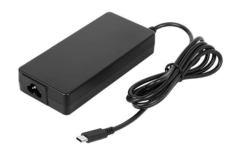
Figure 2: LED Driver picture. Top View
The power supply accepts a wide range input VIN = 108 … 305 VAC and delivers an output VOUT = 20 … 42 VDC. It provides a constant output current of 590 mA in order to keep the individual LED brightness constant, and a maximum output power of 20 W. The LED load current can be selected via firmware. The slow loop bandwidth, with almost constant on-time and switching frequency in steady state operation, allows for very high PF (> 0.9) and low THD (< 20%) from 100% to 50% load. Output ripple is complying with Title 24, JA10, which prescribes a peak-to-average ratio below 30%.
Click image to enlarge
Figure 3: NexGen Vertical GaN JFET in DFN package
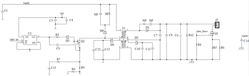
The power processing stage of the converter is depicted in figure 4.
The gate drive circuitry of the power switch is a standard single channel high speed MOSFET driver with the addition of just 3 components: R3 is limiting the DC biasing of the gate below 6 mA, C9 provides negative bias when the device needs to be turned off, together with an instantaneous spike of current at the transitions for faster gate charge removal. D3 negative thermal coefficient (– 2 mV / K typ.) provides for stronger drive at higher temperatures.
Click image to enlarge
Figure 4: Converter power stage schematic. NexGen high voltage switch represented with the designator Q2
Click image to enlarge
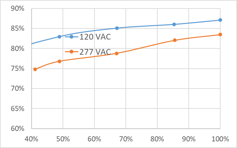
Figure 5: System efficiency in % as function of output current in %. Data taken at 120 VAC and 277 VAC respectively
The traditional R-C-D network across the transformer primary is not populated to reduce BOM cost, power supply volume and maximize efficiency. Worst case steady state Drain voltage stress is around 620 V at VIN = 277 VAC. This is achieved by keeping transformer leakage inductance as low as possible, together with using slow diodes on the primary and secondary auxiliary windings that therefore act as clamping elements. This last technique is generally used to reduce high frequency common mode noise generated by the ringing of the leakage inductance with the primary parasitic capacitance. In this case, the overall improvements are rather limited, given the extremely low value of the power switch output capacitance, as it can be seen by the small leakage spike on the Drain-Source voltage in figures 9 and 11.

Click image to enlarge
Figure 6: Power Factor as function of output current in %. Data taken at 120 VAC and 277 VAC respectively
Click image to enlarge
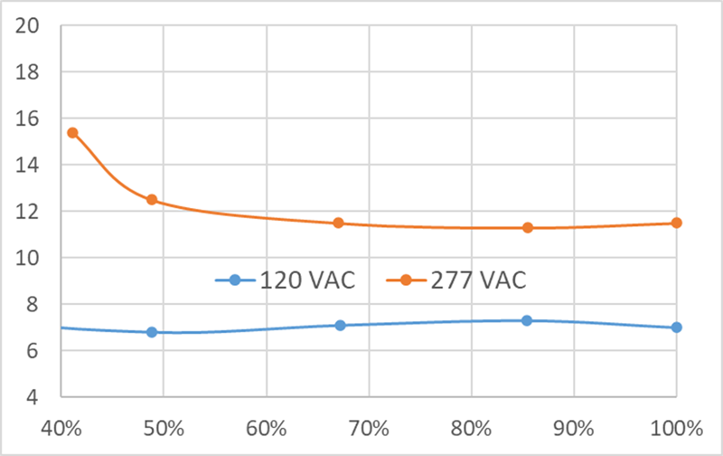
Figure 7: Total Harmonic Distortion in % as function of output current in %. Data taken at 120 VAC and 277 VAC respectively
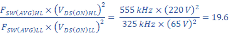
The small transformer used in the design utilized PC200 from TDK as core material: this is specifically designed for high frequency applications and holds its permeability well over a range of several hundreds of kHz. Turns ratio of primary to secondary is Np / Ns = 4, with primary inductance of 250 uH. In this setting, the switching frequency at low line input and full load varies between 230 and 420 kHz which keeps primary current as low as 1.26 A peak and 340 mA RMS. Assuming the thermal drift of the RDS(ON) conduction losses at low line are therefore:

At high line frequency varies between 350 and 760 kHz, primary current is further reduced to 0.98 A peak and 250 mA RMS.

Although conduction losses at high line are 42% lower than at low line, the power switch temperature increase toward ambient in open-frame is 30% higher at high line than it is at low line, with 40°C and 30°C respectively. This is due to the higher switching losses happening at high line. If we just consider the turn-on losses and neglecting Miller capacitance losses, the 220 V maximum turn-on voltage at high line compared to the 65 V at low line, approximately account for a high line to low line ratio of
Total losses in the Vertical GaN device, including conduction and switching components, peak at high line around 500 mW, estimated assuming a junction-to-ambient thermal impedance of 80°C/W.
Overall system performance is described in the graphs in figures 5 to 10. Details on efficiency, Power Factor and Total Harmonic Distortion are provided as function of line and load.
Figures 8 to 11 are oscilloscope screenshots taken while testing the LED driver. Instantaneous switching trends (with some measurement inaccuracies around the input voltage minima) are also shown for reference, with values indicated on the right-hand side of the screen. VDS is the Drain-to-Source voltage on the GaN device, Vsense is the voltage across the 100 mΩ sense resistor in series to the power switch: 100 mV sensed voltage corresponds to 1 A switch current.

Click image to enlarge
Figure 8: Oscilloscope screenshot. VIN = 120 VAC, full load. Trace 2: VDS, 200 V, 1.25 ms / div; trace 3: Vsense, 100 mV / div. Trend 1: instantaneous primary switching frequency (reference legend to the right)
Click image to enlarge
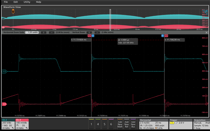
Figure 9: Oscilloscope screenshot. VIN = 120 VAC, full load. Trace 2: VDS, 200 V, 1.25 us / div; trace 3: Vsense, 100 mV / div.

Click image to enlarge
Figure 10: Oscilloscope screenshot. VIN = 230 VAC, full load. Trace 2: VDS, 200 V, 1.25 ms / div; trace 3: Vsense, 100 mV / div. Trend 1: instantaneous primary switching frequency (reference legend to the right)

Click image to enlarge
Figure 11: Oscilloscope screenshot. VIN = 230 VAC, full load. Trace 2: VDS, 200 V, 625 ns / div; trace 3: Vsense, 100 mV / div.
During transients, faults as well as surge, the Drain voltage might approach the 700 V threshold: this event will neither cause permanent damage nor induce a semi-permanent increase to the RDS(ON) of the Vertical GaN switch. The dynamic RDS(ON), well known in the large community of the etero-epitaxially grown GaN devices, is the phenomenon causing a significant increase in RDS(ON) mostly due to the impurity at the interface between different material lattices (GaN grown on Si, on SiC, etc.), which may remain in effect for a few seconds to a few hours, compromising the overall power supply performance and potentially triggering thermal runaways in extreme cases. The RDS(ON) of Vertical GaN devices is not only extremely stable vs voltage but is also best-in-class in regard to temperature dependency: the 1 Ω device used in this LED driver, will increase to around 1.6 Ω at 150°C, a 60% rise, compared to alternative GaN devices experiencing between 70% and 160% in the same temperature range. The immediate effect is the possibility to select a smaller device to work for a given power level, especially in high operating ambient temperature environments. Given the avalanche robustness of the Vertical GaN structure, a Drain voltage temporarily approaching 700 V will just have the switch experiencing slightly higher leakage, with some transient increase in temperature.
Click image to enlarge
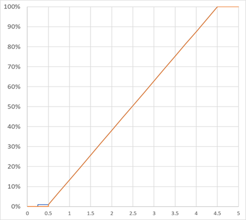
Figure 12: Target LED load current [%] vs analog dimming input [V] characteristic
The LED driver is able to dim from 100% down to 1% in response to an analog dimming input varying from 5 V down to 0.25 V. Below that level, the power supply is entering “light off” mode and this threshold has a 250 mV hysteresis, to avoid flickering at low brightness levels due to noise detected on the analog dimming input. During light-off mode, a deep sleep configuration is entered so that the overall system power consumption can be kept under 500 mW, while still maintaining the necessary house-keeping functionality to guarantee prompt wake-up once the device is required to produce light output again.

Click image to enlarge
Figure 13: Target LED load current [%] vs analog dimming input [V]: zoom-in onto low brightness levels and light off area
The measured dimming profiles (output current in percent vs dimming signal in V) obtained using a 34 V LED string biased at 590 mA with low line and high line input voltages is reported in figure 14. Figure 15 is the dimming profile at 120 VAC and LED string voltage changing between 24 V, 34 V, and 42 V: in this case the LED current is being adjusted via firmware and set in a way that the maximum delivered power is fixed at 20 W (850 mA for the 24 V load, 590 mA for the 34 V load, 480 mA for the 42 V load).

Click image to enlarge
Figure 14: LED load current in percent vs analog dimming input in V. VIN fixed at 120 VAC and 230 VAC

Click image to enlarge
Figure 15: LED load current in percent vs analog dimming input in V. VOUT fixed at 24 V, 34 V, and 42 V. VIN = 120 VAC
A Cortex M0+ processor has been used due to its flexibility. With the resources available, the LED driver can provide multiple maximum current settings and dimming profiles, including linear as well as logarithmic light output reduction. DALI embedded capabilities can be activated via firmware together with fault handling, fault reporting, thermal and power consumption management.
The Helios integrated architecture has all the hooks in place for smart connectivity and IoT applications. Design flexibility and seamless power scalability, uncompromised light quality and highest power per cubic inch will make Vertical GaN the one-stop-shop for present and future LED power modules between 10 W and 200 W.