Leveraging High-Z Technology to Cut Solution Power and Size
Why muxed SAR ADCs equipped with analog input high impedance technology are key to cutting solution size and power, without compromising performance and accuracy.
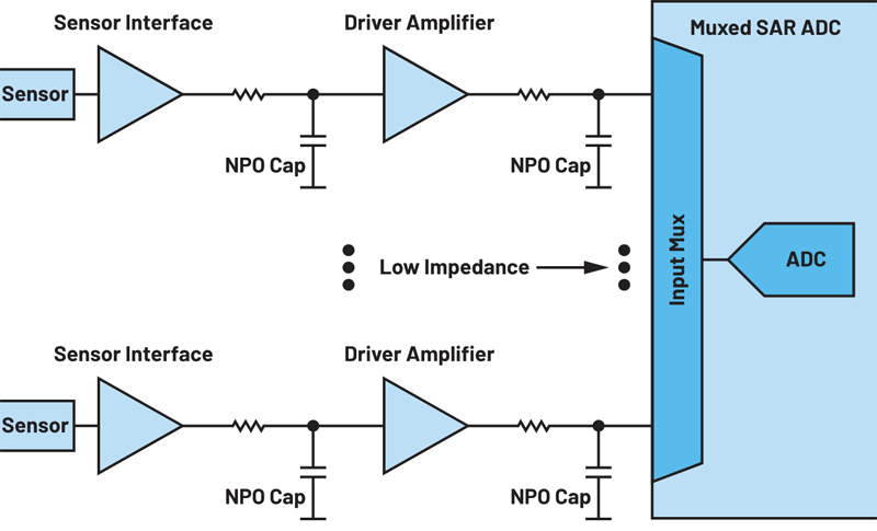
Figure 1. A signal chain with a traditional muxed SAR ADC
Muxed SAR ADCs are commonly used in applications where there is a need to constantly monitor multiple critical variables in the system. In optical communications applications, laser biasing could be monitored via optical power measurement, while EEG/ECG signals from electrodes could be monitored in VSM applications. These muxed applications have some common requirements:
· There are many channels to monitor. Generally, the ADC sequences through all the channels.
· The channel voltages are generally uncorrelated with each other.
· Tight constraints exist on system-level footprint and power.
Some challenges arise because of these requirements. As the ADC finishes a conversion on one channel, the sampling capacitor within the ADC is charged to the voltage of the channel. If this voltage on the sampling capacitor is substantially different from the voltage of the channel next in sequence, then the signal chain must be designed to settle the sampling capacitor to the new voltage accurately, in the allowed acquisition time. Traditionally, the solution to this problem has been to use a wideband driver amplifier, coupled with an RC filter. A typical signal chain is shown in Figure 1.
The sensor could output a voltage or a current, and the sensor interface circuit could be an instrumentation amplifier or a trans-impedance amplifier, respectively. The capacitor is normally an NP0/C0G type, as other types can cause significant distortion. NP0 capacitors have high linearity but low density. The NP0 capacitor is also chosen to be much larger in value than the ADC internal sampling capacitor. It performs two critical functions:
► Reduction of the kickback from the ADC sampling capacitor
► Reduction of the wideband noise of the signal chain by filtering the noise beyond the required settling bandwidth
In the traditional signal chain, one is forced to use a driver amplifier and a large capacitor per channel. Each driver amplifier could consume anywhere between tenths of a mA to a few mA.
Each capacitor, including clearances, could take up around 1mm2 of the board area. Replicating this signal chain over many channels has significant adverse effects on the system footprint and power consumption. This constitutes one of the major problems in muxed SAR ADC applications today.
What Is Input High-Z Technology?
The term high-Z technology, in the context of analog input, refers to a collection of circuit techniques that—without consuming static or continuous power — substantially increase the effective input impedance of the ADC. This makes the input of the ADC easy to drive.
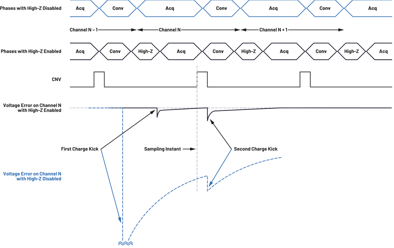
Let’s assume that the muxed ADC is converting on Channel N–1 and that the next channel to be converted is Channel N.
At the rising edge of convert start (CNV), the channel voltage is sampled. In Figure 2, the first rising edge of CNV samples the voltage on Channel N – 1. The ADC then converts the sampled voltage on Channel N–1. After the conversion, with the input high-Z disabled, the ADC proceeds to acquire the next channel in the sequence, which is Channel N. The voltage on Channel N can often be substantially different from the voltage on Channel N – 1, to which the ADC capacitor is now charged. This results in a huge voltage kick on Channel N (dark blue dashed line) and introduces a large error in the channel voltage at the sampling instant (second rising edge of CNV). This necessitates a large external capacitor to absorb the kick and a driver amplifier to supply the necessary charge.
Click image to enlarge
Figure 2. Phases of the AD4696 with high-Z enabled and disabled
When the input high-Z is enabled, the internal sampling capacitor of the ADC ischarged up to the present voltage on the channel it is going to acquire before it begins the real acquisition. Immediately following the conversion on Channel N–1, a high-Z phase is introduced that accurately charges the ADC sampling capacitor to the present voltage on Channel N. This means that when the ADC sampling capacitor does connect to the external input, it doesn’t source any charge and doesn’t result in any kickback. In practice, there is usually a small residual error due to the charge injection of the internal switches (first charge kick). This small residual error results in practically negligible settling error at the sampling instant of Channel N. This charge error with the high-Z enabled would enable a massive improvement in the settling dynamics of the system.
When the sampling on Channel N is done, the ADC must proceed to do the conversion. So, the internal switches disconnect the ADC sampling capacitor from the external input. This results in a second charge kick due to the switch opening charge injection. Typically, the second charge kick has longer time to settle, so the magnitude of the first charge kick determines the settling error on a channel. Therefore, the first charge kick magnitude must be minimized.
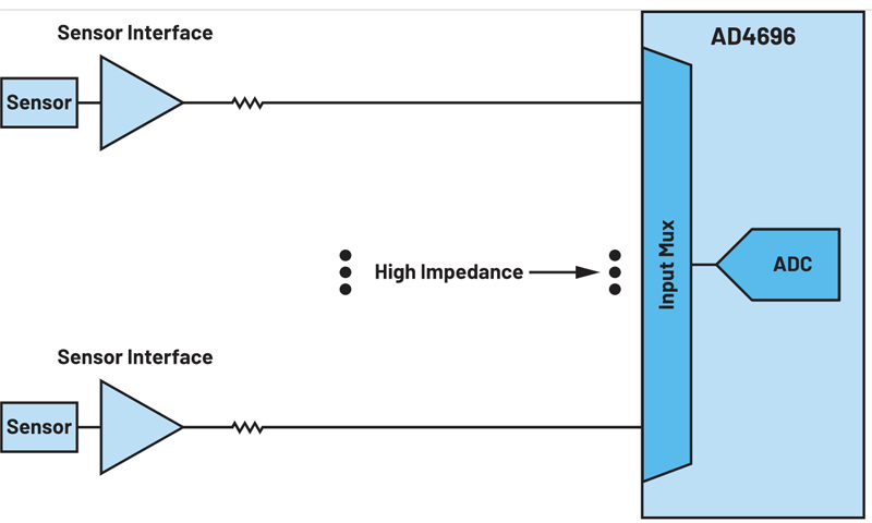
The input high-Z technology is incorporated in the AD4696 (latest generation muxed SAR ADC) as part of the Easy Drive feature set. As a result, the AD4696 begins acquisition on a channel extremely smoothly. It eliminates the need for a kickback absorption capacitor and a driver amplifier for each channel. This results in the massive reduction of the system footprint and power consumption, as well as a significant simplification of the signal chain, as shown in Figure 3.
Click image to enlarge
Figure 3. A signal chain with the AD4696 muxed SAR ADC
An important advantage of the input high-Z implemented in the AD4696 family is that the circuits that perform the high-Z function can all be power cycled at the rate of the conversion. So, the power consumption of the high-Z function would scale linearly with the throughput of the ADC, just like the core SAR ADC itself. This offers remarkable flexibility compared to the traditional, rather rigid signal chaindesigns.
The input high-Z function is also built into the LTspice model of the AD4696. The first and second charge kicks are accurately modeled, enabling reliable simulation of the settling artefacts for signal chain designs.
Some Subtleties
Recall that the NP0 capacitor also provided wideband noise filtering of the signal chain. Now that we want to eliminate the capacitor, we must find other ways to filter the noise. A simple way to achieve the same effective signal chain noise bandwidth is to increase the external series resistance. The AD4696 has a 60 pF internal capacitor in series with a 240 Ω typical internal resistor. By setting the external resistor, we can tune the signal chain noise bandwidth to a desired value.
Without the NP0 capacitor, the external resistance plays an important role in the noise performance, linearity, and accuracy of the signal chain. A small value resistor can help settle sampling charge kicks quickly and thus improve linearity and accuracy, but it comes at the cost of increased overall noise due to higher effective noise bandwidth. Conversely, a large value resistor filters noise better, but it comes at the expense of degraded linearity and accuracy.
As described in the next section, a big advantage of the high-Z technology in AD4696 is that it allows large value resistors to be used (for better noise filtering) without degrading the linearity and accuracy. This allows optimization for all parameters in the signal chain — noise, linearity, accuracy, power, and solution size.
Measurement Results
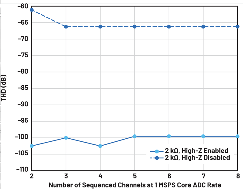
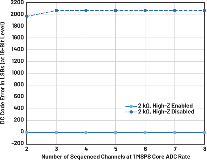
Measurements have been performed with a 2 kΩ external resistor and without any NP0 capacitor. The results show a massive improvement in AC and DC performance with the analog input high-Z enabled. The experiment involves running the core ADC of AD4696 at 1 MSPS but choosing an increasing number of channels as part of around-robin sequence. Data are collected on one channel, while the other channels in the sequence are provided with 0 V inputs.
Figure 4 shows the distortion performance of the channel of interest for a 1 kHz,–1 dBFS tone. As the channels are sequenced with the high-Z disabled, nonlinear settling errors occur because the sampling capacitor is not charged to the subsequent channel voltage. This results in significant distortion. With the high-Z enabled, there is a massive improvement in the distortion performance.
Click image to enlarge
Figure 4. THD vs. number of channels in a sequence. Test tone: 1 kHz, –1 dBFS
Figure 5 shows the DC steady-state settling errors with and without the high-Z function. In this test, the channel of interest is provided with a near full-scale input and the other channels in the sequence are driven with 0V. Conversions are performed on the channel of interest while adding an increasing number of channels to the sequence, and the shift in the average output code from the expected code is plotted.
Click image to enlarge
Figure 5. DC settling errors in LSBs at 16-bit level
When operating the core ADC at lower throughputs than 1 MSPS, the user may need to further lower the effective signal chain noise bandwidth to limit the analog front-end noise aliasing. This would necessitate higher resistance values, and the high-Z function helps immensely with maintaining the performance under these conditions.


