Using Planar Flyback Transformers to Meet Increasing Efficiency Requirements in High Voltage Applications
There is a growing importance to improve industrial power supply electrical efficiencies that is being driven by environment and economic factors. Even a small efficiency enhancement can translate into energy reductions that lead to costs savings and more productive and, many times, more reliable and longer lifespan applications. Challenging power efficiency advancements are today’s more integrated designs that bundle an increasing amount of functionality into smaller and smaller form factors.
To convert electrical power, AC/DC power supplies of less than 100W typically use flyback topologies mostly because they are the simplest and lowest cost of all isolated topologies. Planar magnetics are commonly the high-frequency application converter of choice due to their low resistance and minimal number of turns in helical windings. Planar transformers also deliver a number advantages for high voltage applications such as offering a lower mechanical profile for space-constrained designs. Along with the benefits are several technical challenges to overcome that include design considerations for high inductance values and the level of isolation needed for safety reasons. The good news is that there are suppliers with the expertise to offer customized planar flyback transformer designs that have been tested to deliver peak efficiencies of over 90 percent.
Advantages Gained; Disadvantages to Overcome
Planar transformers offer advantages over wound transformers in that their cores have wider surface areas than traditional E, EC or EP cores to permit a smaller number of turns in the windings. The wider core areas also enable lower DC resistance of the copper.
Furthermore, the rigid structure of the planar transformer’s PCB (standard thickness 1.3mm) eliminates the need for a plastic carrier or bobbin so it provides a thinner and lower profile solution versus a wound transformer. Another benefit is the simplified manufacturability of a PCB that also enables higher tolerances in transformer specifications such as inductance, resistance and turns ratios.
There are disadvantages that must be overcome as well. PCB substrates like FR4 don’t typically meet safety requirements for insulation in high voltage applications. Differential surges can also jump across from vias to cores causing damage. Also, implementing multiple layers can be problematic in the design phase and expensive especially if thick copper plating is required.
Designing for Maximum Efficiency
Using a USB power delivery system as an example, a custom planar flyback transformer can be designed to deliver up to 100 W (20V, 5A) with the understanding that a continuous conduction mode is recommended for powers greater than 10 W. This design avoids very peak currents that can cause high switching losses and overheating of the core. In this solution, the main contributing factor to losses will be from the copper and not the core, and was designed with a primary inductance value of 530uH to keep peak currents under 2.3A so as to not overstress the external 650V MOSFET. It uses 30 turns on the primary side calculated based on the saturation current, inductance value and area of the core (EC26).
The design uses 12-layer winding that incorporated a primary and secondary winding produced using 2-ounce copper, FR4 PCB material and two identical substrates. The transformer’s PCB forms a split primary winding enclosing the secondary made from triple insulated wire (Figure 1). The triple insulated wire on the secondary side provides the reinforced insulation between primary and secondary windings. As the design uses just four turns, it fits in a spiral shape around the core and between the two PCBs.
Reducing Core Loss and Leakage Inductance
The flux density is highest at the edge of the core so the flux must travel through the side wall of the core to complete its path. Therefore, the flux density will increase at the side. However, the flux density in the center leg is well below saturation (Shown in Figure 2).
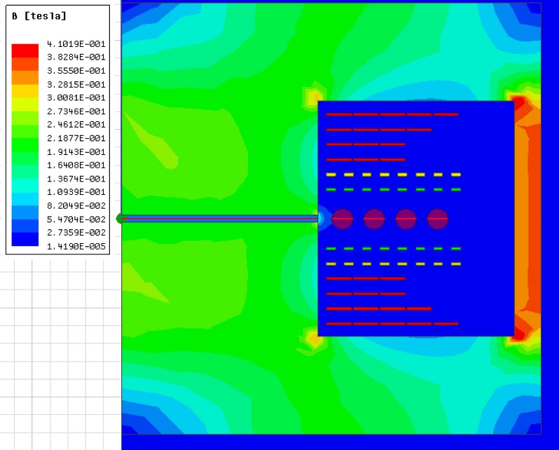
Click image to enlarge
Figure 2. Flux density in the transformer using 2D FEA.
Leakage inductance is a source of energy waste and must be kept to a minimum to increase overall efficiency. The leakage inductance value depends on the magnetic field between the primary and secondary winding. According to Amperes Law, the ampere turns across the interwinding region is the same as the ampere turns in either winding so the winding width was kept at a maximum to reduce the field strength in this region.
In addition, the volume of the interwinding region was kept as small as possible to reduce leakage. Increasing the winding breadth also reduces leakage inductance. The effective winding breadth was increased by interleaving the layers. This design had four turns on the secondary implemented using a single layer insulated wire. This eliminates the need for creepage and clearance distances between primary and secondary windings. The secondary was interleaved with the primary, which effectively doubles the winding breadth of the primary cutting the leakage inductance value in half.
The interwinding volume is better controlled if the secondary is also implemented in PCB material. Though using insulated wire on the secondary removes the need for creepage and clearance distances between the primary and secondary windings. This is particularly important in high voltage applications. Furthermore, interwinding capacitance is adversely affected if their distances are decreased, and is serious for high voltage applications as it worsens the coupling of AC power line noise through to the power supply output.
The leakage inductance on the custom planar flyback transformer was recorded as 14uH at 130kHz by shorting the secondary wire and measuring the primary inductance.
Controlling AC Losses
In a flyback transformer, there is no benefit to the AC resistance in interleaving the primary and secondary as these windings are out of phase. The AC resistance on the primary side can be controlled by keeping the copper at less than the skin depth at the switching frequency. The skin depth in this transformer is 0.2mm while the thickness of copper is 0.07mm.
At maximum load, the secondary AC current is 7.3A due to the pulsating nature of current on the secondary side. This would lead to copper losses of 1.5W on the secondary side due to the 0.8 mm diameter of the wire. Finite element analysis (FEA) analysis shows the conductor closest to the gap experienced a hot spot due to the high circulating AC currents and eddy currents induced by fringing effects.
To reduce the copper losses at high frequencies, the insulated secondary wire would have to be replaced with a helical winding. And because the FR4 PCB material is not considered safe, a barrier such as mylar or polyimide tape needed to be bonded to the PCB substrate.
AC/DC Adaptor Application Example
The custom planar flyback transformer was tested on a AC/DC adaptor shown in Figure 3. The design is based on a Discontinuous Conduction Mode (DCM) Flyback Converter topology with valley switching and synchronous rectification. Both the valley switching and synchronous rectification reduce power losses in the external MOSFET and rectifier respectively. Operating in DCM mode meant that there would be zero ampere turns in the transformer for a period every switching cycle.
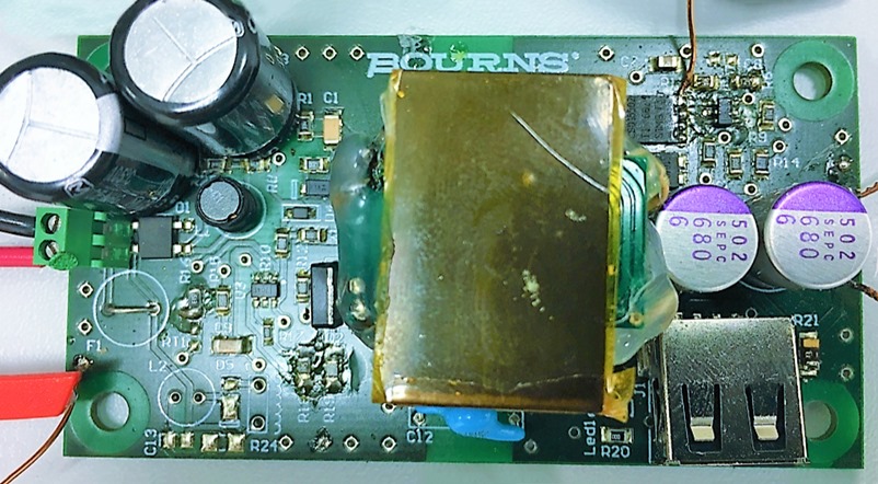
Click image to enlarge
Figure 3. View of an AC/DC adaptor with a planar flyback transformer.
The operating mode of the transformer is shown by the voltage across the drain of the MOSFET. The voltage across the drain consists of the bulk voltage across the primary plus the reflected output voltage from the secondary. However, once the secondary current reaches zero there are no more ampere turns in the windings meaning that the mutual inductance collapses. This leads to a period of oscillation around the bulk input voltage. The controller IC senses this from the auxiliary voltage and switches off the synchronous rectifier to save energy. If the load is increased, this period of resonance is reduced until it disappears and the converter passes into continuous conduction mode.
In this example, the power supply operated at 115V AC input with a 5V output. Bourns measured the efficiency at different output powers. The testing showed the biggest loss came from the snubber diode, which was the hottest component reaching 51°.3C. Optimizing the snubber resistor value and reduction of the leakage inductance in the transformer helped improve power loss in this area.
Efficiencies Achieved
This example illustrated that planar magnetics can be optimal conversion solutions for high frequency, high current applications including high voltage AC/DC adaptors while also delivering low profile design advantages combined with PCB construction for high-quality manufacturing.
Bourns designed this planar transformer with reinforced insulation, created by splitting the primary into two PCBs and sandwiching a four-turn secondary using triple insulated wire providing a necessary barrier between primary and secondary. Reducing the leakage inductance, Bourns split the primary resulting in a leakage reduction of 50%. Using this structure and testing it on a AC/DC flyback in DCM mode with 5V output provided a peak efficiency of 91.05% in the test conducted by Bourns.