GaN switches need careful design of their gate drive circuit to achieve the promised gains in efficiency and power density with operational reliability
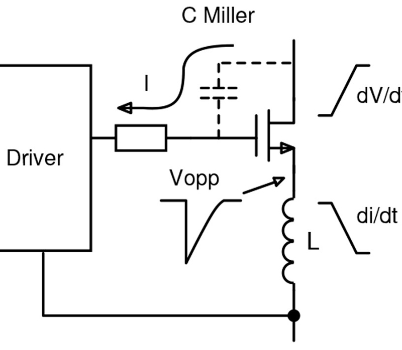
Figure 1: Inductance common to source and gate drive causes voltage transients
Gallium Nitride (GaN) HEMT is the enabler for demonstrations of power converters with end-to-end efficiencies greater than today silicon-based solution, comfortably exceeding the most stringent 80+ spec for server and cloud data center or EU Code of Conduct Tier 2 standard for USB PD external adapter. While older silicon-based switch technologies have claimed performance close to the ideal, with fast, low-loss switching, GaN devices are closer still - but not as drop-in replacements. To get the full potential benefit of the technology, the external drive circuit has to be matched to the GaN device, along with careful board layout.
Comparing GaN and silicon switches
Higher efficiency is the headline potential benefit of enhancement mode GaN compared with Silicon (Si) switches. Unlike its depletion mode counterpart, enhancement mode GaN is a normally OFF device so it requires a positive gate drive voltage to switch the device ON. Higher efficiency of enhancement mode GaN stems from lower device capacitances and GaN’s ability to conduct in the reverse direction (third quadrant) but with zero reverse recovery charge; a major benefit in ‘hard-switched’ applications. Low gate-source and gate-drain capacitance yielding low total gate charge allows for rapid gate switching and low dissipation in the gate driver. Also, low output capacitance gives low turn-off losses. Other differences that can compromise practical GaN performance, though, are the lack of drain-source/gate avalanche voltage rating and a relatively low absolute maximum gate voltage, typically only +/-10V compared with Si MOSFETs at around +/-20V. In addition, turn-on threshold (VGTH) for GaN, at around 1.5V, is much lower than a Si MOSFET, which is around 3.5V. If the external drive and load circuit can be managed to control source and gate voltages reliably, switching frequency can be pushed into several hundreds of kHz or MHz region, maintaining high efficiency with consequent reduction in magnetic and capacitor component sizes yielding dramatic W/in3 power densities.
GaN gate drive is key to performance
Keeping gate drive voltages within absolute maximum limits is not the only requirement. For fastest switching, a typical GaN device needs to be driven to an optimum VG(ON) value of around +5.2V for full enhancement without a penalty in excessive gate drive power. Driver power PD is given by:

Where VSW is the total gate voltage swing, f is switching frequency and QGTOT, the total gate charge. Although the GaN gate is effectively capacitive, the power is dissipated in the gate effective series resistance and driver. Keeping the voltage swing minimum is therefore important, especially when the frequency is very high. QGTOT is typically a few nC for GaN, around a tenth of the value for a similarly rated Si-MOSFET - one of the reasons why GaN can switch so fast. GaN devices are charge-controlled so for nanosecond switching with nanocoulomb gate charge, peak current is in the order of an amp, which must be provided by the driver while maintaining accurate voltage.
In theory, GaN devices are securely off with VGS = 0, but in the real world, even the best of gate drivers may not apply 0V directly to the gate. Any series inductance L, in the source lead that is common to the gate drive loop will generate an opposing voltage VOPP to the gate drive, which can cause spurious turn-on with high source di/dt, according to VOPP = -L di/dt (figure 1). The same effect can be caused by the off-state dV/dt forcing current through the device ‘Miller’ capacitance, but for GaN this can be negligible. A solution is to provide a negative gate off-voltage of perhaps -2 or -3V, but this complicates the gate drive circuit and can be avoided with careful board layout and use of devices with ‘Kelvin connections’ and minimal package inductance, such as the low profile, leadless PQFN type.
High-side gate drives present their own challenges
GaN devices are not necessarily optimum for all topologies, such as most ‘single-ended’ Flyback and Forward types where reverse conduction does not occur and the extra cost over Si-MOSFETs outweighs any small efficiency benefit. However, ‘half-bridge’ topologies – such as Totem-Pole Bridgeless PFC’, LLC converters and Active Clamp Flyback – will be a natural home for GaN, whether hard- or soft-switched. These topologies all have ‘high-side’ switches where its source is a switching node, so the gate drive is offset from ground by a high-voltage and high-frequency waveform with nanosecond-scale edges. The gate drive signal originates from a controller referenced to system ground, so the high-side driver must incorporate level shifting with the appropriate voltage-withstand rating typically 450 V or higher. It also needs a means of generating a low-voltage power rail for the high side drive, typically with a network of bootstrap diode and capacitor, referenced to the switching node. The switching waveform stresses the driver with dV/dt; with GaN, that figure can be over 100V/ns. This induces displacement current through the driver to ground, potentially causing transient voltages across series resistances and connection inductances that could corrupt the sensitive differential gate drive voltage. The driver should therefore have strong dV/dt immunity.
For maximum immunity to catastrophic ‘shoot-through’ and best efficiency, half-bridge high- and low-side devices should be driven with a guarantee of no overlap while keeping dead-time to a minimum. The high- and low-side drivers should therefore have very well controlled and matched propagation delays.
For the low side, the driver ground should be connected directly at the switch source for a Kelvin connection to avoid common inductance. This can be a problem as the driver also has a signal ground, which may not be best connected at this point. Because of this, the low side driver may feature isolation or some method of splitting power and signal grounds with a degree of common-mode voltage tolerance.
GaN drivers may need safety isolation
Enhancement mode GaN devices are receiving the greatest attention todays for offline application that requires high voltage rating of at least 600 V for both the device and its driver although lower voltage applications are increasingly common. If the driver input signals are generated by a controller with human-accessible connections, perhaps through communications interfaces, the driver will require safety isolation complying with the relevant codes. This can be achieved with high speed signal galvanic isolator with appropriate insulation voltage. Maintaining driver signal edge rates and high- and low-side matching becomes problematic with these arrangements, although the controller circuitry is often allowed to be ‘primary-referenced’ as is normal anyway in most case of AC-DC converters.
Application example - ‘active clamp flyback’
This is an example of an active clamp flyback topology (Figure 2), that uses a high-side switch to recirculate energy back to the supply from the leakage inductance in the converter transformer. Compared with the ‘snubber’ or hard zener clamp approach, efficiency is higher, EMI better and the drain waveform is cleaner, with the circuit having applications at low power between 45 W to 150 W. Typical applications include travel adapters for cell phone and laptop that are USB PD enabled, as well as embedded power supplies.
In Figure 2, an ON Semiconductor NCP51820 dedicated GaN gate driver [1] is shown with a NCP1568 [2] active clamp flyback controller (detail omitted). The driver features gate drivers with regulated +5.2V amplitude for both high side and low side optimum for enhancement mode GaN. It also has -3.5V to +650V high-side common-mode voltage range with -3.5 to +3.5V for the low side and 200V/ns dv/dt immunity, enabled by an advanced junction-isolation technology. Having level shifting for the low-side drive makes Kelvin connection easier if there is a current sense resistor in the low-side device source. Driver waveform rise and fall times are 1ns, with a maximum propagation delay of 50ns and separate source and sink outputs are provided for the high and low sides to enable tailoring of gate drive edges for best EMI/efficiency trade-off. In this topology, the high and low side drives do not overlap but have differing pulse widths to achieve power conversion/regulation with drain clamping and zero-voltage switching, controlled by the NCP1568 device.
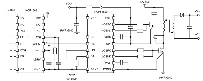
Click image to enlarge
Figure 2: GaN based active clamp flyback converter outline
Application example – LLC converter
At higher power above 150 W, a resonant LLC converter is often used for its efficiency and limited voltage stress on the switches. A feature of the converter is that drive waveforms are each 50% duty cycle with regulation achieved by varying frequency. It is vital therefore that dead time is controlled to guarantee no overlap occurs. Figure 3 shows a typical arrangement with NCP13992 high performance LLC controller. Such design can be operated at 500 kHz switching frequency and is typically employed in high power gaming adapters and embedded power supplies for OLED TV and All In One PC.
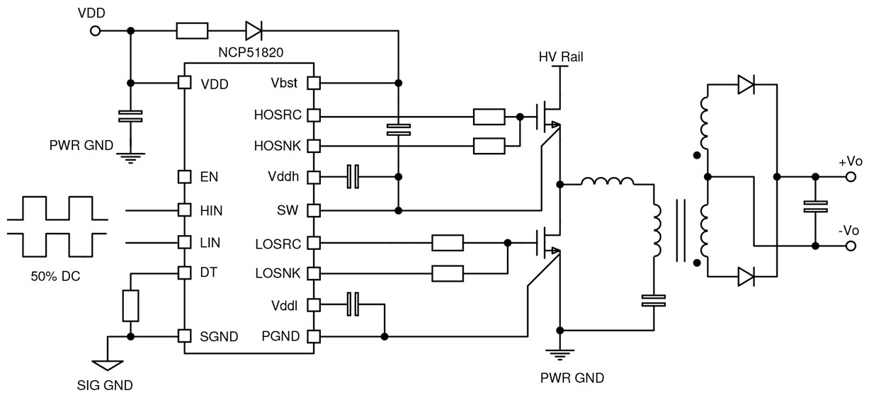
Click image to enlarge
Figure 3: GaN based LLC converter outline
The ON Semiconductor NCP51820 driver illustrated provides the guarantee that the gate drives cannot overlap, although this can be disabled for topologies that require it (such as current-fed converters). The device also includes an enable input and comprehensive protection against supply under-voltage and overtemperature. It is available in a PQFN, 4 x 4mm 15-lead package enabling short, low inductance connections to the gates of the GaN devices.
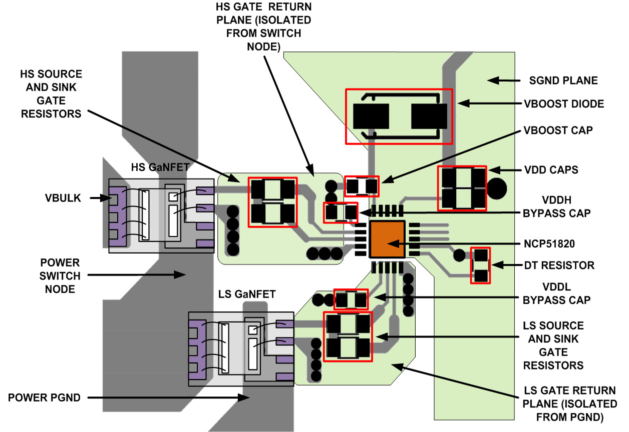
Board layout considerations
In all applications, board layout is critical for success. Figure 4shows an example layout with the On Semiconductor NCP51820 that minimizes and matches the gate driver loop. GaN devices and driver are placed on the same PCB side to avoid high current through vias with appropriate use of ground/return planes.
Click image to enlarge
Figure 4: Good layout practice for GaN gate drive circuitry
On Semiconductor