Providing high efficiency over the entire load range
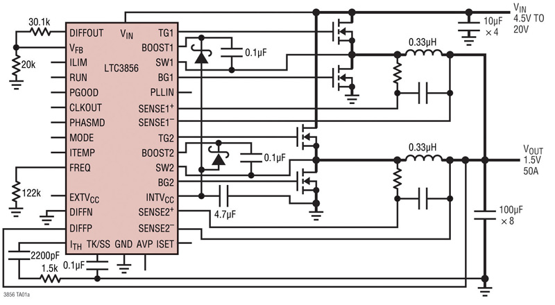
Figure 1: High output current 1.5V/50A application schematic
The data centers' incremental overhead power consumption, due to inefficiencies and cooling systems is estimated to be equal to the amount of power that is consumed by servers, storage and networking. The user of a single PC, workstation, or laptop doesn't see system heat generation as a concern, but for data centers, managing this thermal overhead is as important as the servers themselves. If system power is reduced, then the available overhead can handle a greater IT load and perform more useful work in the same power envelope. As the data center power demand continues to increase, higher efficiency power conversion is required to reduce the amount of power wasted as heat. Smart multiphase controller technology is an excellent solution for high current POL applications. This architecture allows a high current regulator to achieve well over 90 percent efficiency at full load. However, most designs do not address the need for higher efficiency at light to medium loads. Wasted power at a light to medium load is just as important to save as wasted power at heavy loads. Most embedded systems are powered via a 48V backplane. This voltage is normally stepped down to a lower intermediate bus voltage of 24V, 12V or 5V to power the racks of boards within the system. However, most of the sub-circuits or ICs on these boards are required to operate at voltages ranging from sub-1V to 3.3V at currents ranging from tens of milliamps to hundreds of amps. As a result, point-of-load DC/DC converters are necessary to step down from either of the 24V, 12V or 5V voltage rails to the desired voltage and current level required by the sub-circuits or ICs. It is clear that the growing demand for increased current at ever decreasing voltages is driving power-supply development. Much of the progress in this area can be traced to gains made in power conversion technology, particularly improvements in power ICs and power semiconductors. In general, these components contribute to enhancing power supply performance by permitting increased switching frequencies with minimal impact on power-conversion efficiency. This is made possible by reducing switching and on-state losses thereby increasing efficiency while allowing for the efficient removal of heat. However, the migration to lower output voltages places more pressure on these factors, which in turn, creates significant design challenges. Multiphase Topology Multiphase operation is a general term for conversion topologies where a single input is processed by two or more converters, where the converters are run synchronously with each other but in different, locked phases. This approach reduces the input ripple current, the output ripple voltage and the overall RFI (radio frequency interference) signature, while allowing high current single outputs, or multiple lower current outputs with fully regulated output voltages. It also allows smaller external components to be used, producing a higher efficiency converter and also providing the added benefit of improved thermal management with less cooling. Multiphase topologies can be configured as step-down (buck), step-up (boost) and even as a forward converter, although generally the buck regulator is the more prevalent application. Conversion efficiencies of up to 95% from 12V in to 1.xV out are commonplace today. At higher power levels, scalable multiphase controllers reduce the size and cost of capacitors and inductors using input and output ripple current cancellation caused by interleaving the clock signals of several paralleled power stages. Multiphase converters help minimize the external component count and simplify the complete power supply design by integrating PWM (pulse width modulation) current mode controllers, true remote sensing, selectable phasing control, inherent current sharing capability, high current MOSFET drivers plus overvoltage and overcurrent protection features. The resulting manufacturing simplicity not only helps improve power supply reliability, but it is also scalable. Such systems can be expanded up to 12 phases for high current outputs as high as 300A. Linear Technology has several multiphase DC/DC controllers, including the LTC3856 and LTC3829 single output synchronous step-down controllers for high current POL conversion. Not only can these parts increase full load efficiency, but they also have an optional Stage Shedding™ feature that decreases light to medium load power loss as well. The circuit in Figure 1 shows a typical LTC3856 application schematic for developing a 1.5V/50A output from a 4.5V to 14V input voltage using two phases.
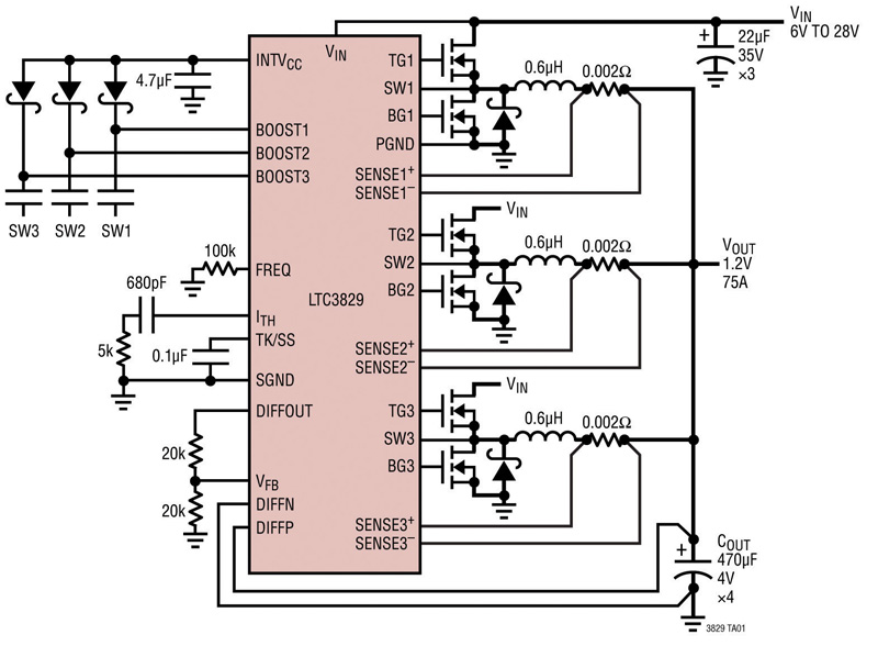
The circuit in Figure 2 shows a typical LTC3829 application schematic for developing a 1.2V/75A output from a 6V to 28V input voltage with three phases. The LTC3856 has two channels and up to 12 phases possible with multiple ICs. The LTC3829 has three channels and can operate at up to 6 phases when used with two ICs. The onboard differential amplifier provides true remote output voltage sensing of both the positive and negative terminals, enabling high accuracy regulation independent of IR losses in trace runs, vias and interconnects. Additional Benefits These controllers operate with all N-channel MOSFETs from input voltages ranging from 4.5V to 38V, and can produce ± 0.75% accurate output voltages from 0.6V to 5V. The output current is sensed, monitoring the voltage drop across the output inductor (DCR) for highest efficiency or by using a sense resistor. Programmable DCR temperature compensation maintains an accurate over current limit set point over a broad temperature range. The powerful onboard gate drivers minimize MOSFET switching losses and allow the use of multiple MOSFETs connected in parallel. A fixed operating frequency can be programmed from 250kHz to 770kHz or synchronized to an external clock with its internal PLL. A minimum on time of just 90ns makes the LTC3729 and LTC3856 ideal for high step-down ratio/high frequency applications.
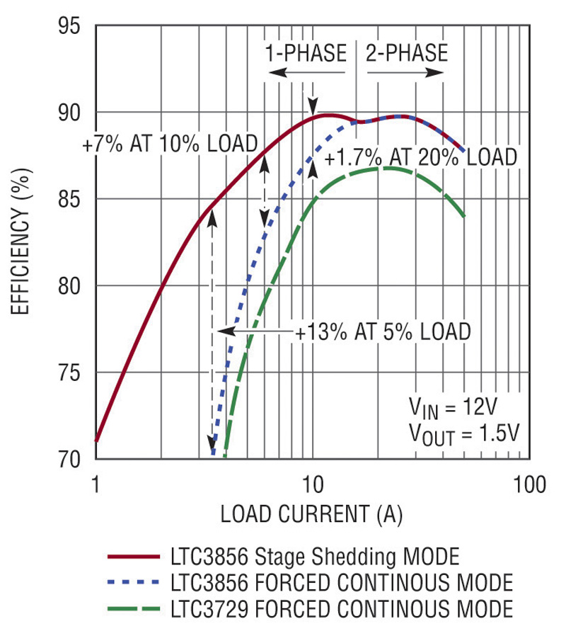
Stage Shedding Operation At light loads, switching-related power losses normally dominate the total loss of a switching regulator. Eliminating the gate charge and switching losses of one or more of the output stages during a light load will significantly increase efficiency. Stage Shedding allows one or more phases to be shut down to reduce switching related losses during a light load condition and is typically used when the load current is reduced to less than 15 amps. The overall efficiency can be increased by up to 13%, as shown in Figure 3. This figure also shows the efficiency of an older comparable LTC3729 2-phase controller. Due to the stronger gate drive and shorter dead time, the LTC3856 can achieve 3-4% greater efficiency than the LTC3729 over the whole load range.
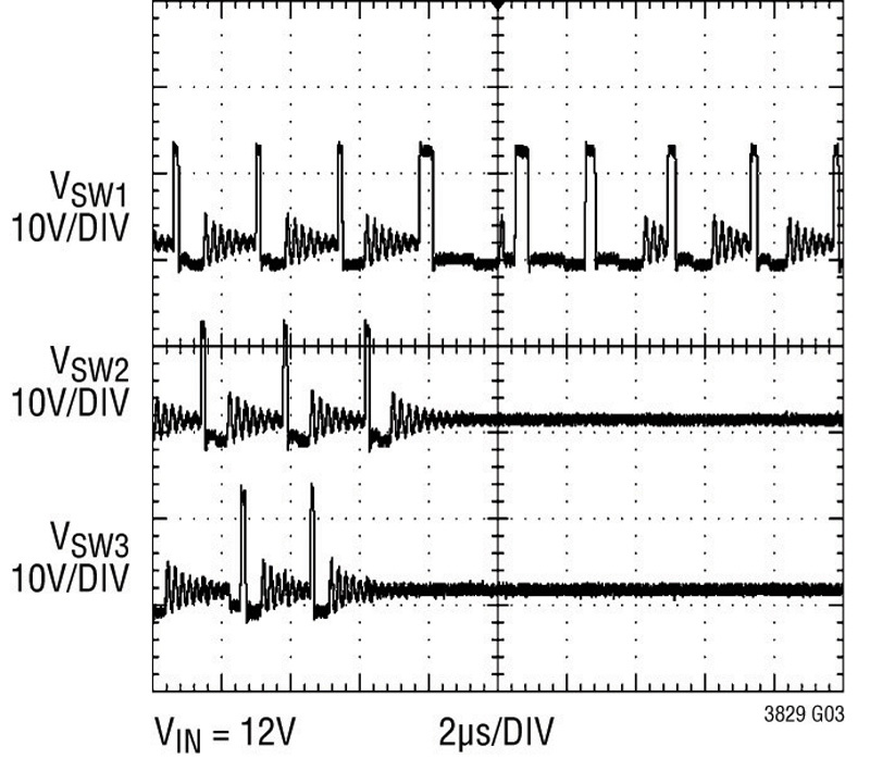
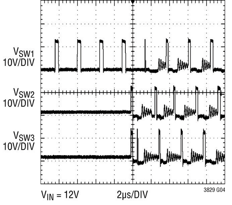
Stage shedding operation is triggered when the onboard feedback error amplifier output voltage reaches a user-programmable voltage. At this programmed voltage, the controller shuts down one or more of its phases and stops the power MOSFETs from switching on and off. This ability to program when Stage Shedding takes place provides the flexibility to determine when to enter this mode of operation. The diagrams in Figure 4 show the SW waveform and how the LTC3829 goes into and out of Stage Shedding operation.
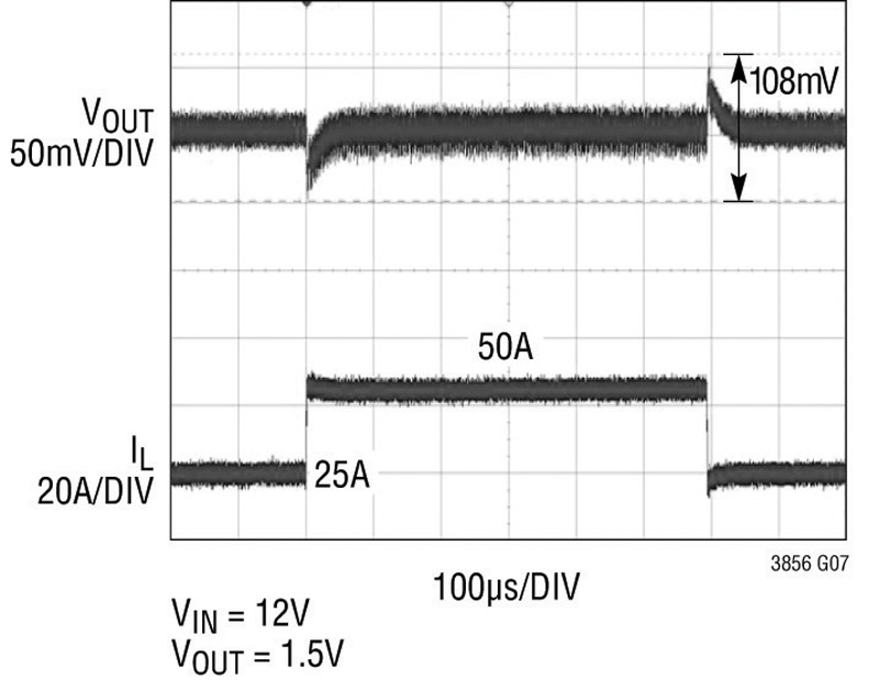
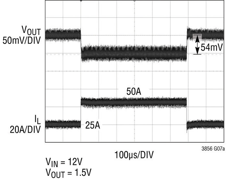
The LTC3856 and LTC3829 can operate in any of three modes: Burst Mode® operation, forced continuous or Stage Shedding mode, all of which are user selectable. At heavy loads of greater than 15 amps, these devices operate in constant frequency PWM mode. At very light loads, Burst Mode operation can be selected and produces the highest efficiency at load currents of less than 0.5A. Burst Mode operation switches in pulse trains of one to several cycles, with the output capacitors supplying energy during internal sleep periods. Active Voltage Positioning The LTC3856 and LTC3829 also have Active Voltage Positioning (AVP), which reduces the maximum voltage deviation during a step load and reduces the power dissipation at heavier loads further increasing its efficiency. Figure 5 shows the difference in behavior between the circuit in Figure 1 with and without AVP. Without AVP, the maximum voltage deviation for a 25A step load is 108mV. With AVP, the maximum voltage deviation is 54mV for the same 25A step load. In addition, the output voltage drops by 54mV with AVP when the output current goes from 25A to 50A, resulting in a lower 2.7W dissipation by the load.
Conclusion The need to reduce the power dissipation in data centers will be a major focus for the next several years. Designers of POL DC/DC converters for almost any kind of system face many challenges due to the multiple constraints of limited space and cooling within a given enclosure, as well as the need for high efficiency throughout the entire load range. Despite having to navigate through this myriad of constraints, many of the recently introduced multiphase regulators provide a simple, compact and efficient solution. By moving toward the diverse multiphase topologies, designers can effectively save space, simplify layout, lower capacitor ripple current, improve reliability and reduce the amount of power wasted as heat. www.linear.com