In the continuous efforts to improve power conversion efficiency, wide band-gap semiconductors are enabling significant advances
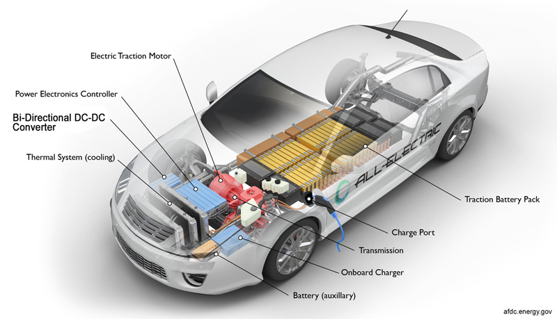
Figure 1: Typical EV power conversion elements
Ask any power electronics designer what they strive for and top of the list is normally conversion efficiency. It’s not just for energy savings but also the knock-on benefits of smaller, lighter and cheaper products, with options opening up for better reliability and more functionality in space that’s freed-up. Some applications particularly benefit, such as EVs, where range can be enhanced and in server farms, where energy consumption of electronics and necessary air conditioning is a major issue, currently over 1% of total global demand.
Viability of EVs is driven by power conversion efficiency
An EV is a data center on wheels, with industrial-scale motor control alongside (Figure 1) and its very viability depends on the efficiency of the traction inverter and charging circuitry. Every percentage point improved is part of a virtuous circle of less heatsinking required, lower weight and longer range at lower cost.
At an EV’s heart, the lithium-ion battery can be 48V for a mild hybrid and up to 500-800V for a full electric version. There is an on-board AC-DC charger, often bi-directional to return excess energy to the grid for credit, various auxiliary DC-DC converters to power comfort and safety equipment and, of course, the traction inverter, again with bi-directional energy flow to harness regenerative energy from braking or free-wheeling.
The semiconductor switches in EV power conversion overwhelmingly set the losses, and for the traction inverter, IGBTs might be a natural choice, although they can only switch efficiently at low frequencies. This has not previously been a major issue however, as the AC motors operate adequately at 10kHz drive or less. There are though benefits to increasing the frequency somewhat, with smoother motor control and a more sinusoidal drive achievable, with consequent lower iron losses and motor wear. Conduction losses of IGBTs are kept low by a near constant saturation voltage, but wide band-gap switches, particularly in silicon carbide (SiC) are appearing with such low on-resistance that they are now competitive, and can be paralleled at will for even lower losses. SiC devices as FETs or MOSFETs also match the requirement for bi-directional energy flow, as they can conduct in either direction, configured as either switches or synchronous rectifiers. IGBTs don’t conduct in reverse and need a lossy parallel diode to achieve the same function.
EV Chargers and auxiliary DC-DC converters also increasingly form part of the energy loss equation as power demand increases and these directly benefit from higher frequency switching with small magnetics. Silicon super-junction MOSFETs have been a traditional choice for switches but useful efficiency gains are now attainable with wide band-gap devices with their faster edge rates and downward trend in on-resistance.
New power conversion topologies maximize efficiency in data centers
Although energy demand in data centers gets ever-heavier, the introduction of high efficiency power converters and distribution schemes has actually held the increase to only around 6% from 2010 to 2018, even though internet traffic increased 10x and storage 20x in the same period.
AC-DC Converters in server farms now routinely achieve ‘80+ Titanium’ standards: 96% minimum efficiency at 50% load, 230VAC, facilitated by high-efficiency topologies such as the ‘bridgeless totem-pole’ PFC stage (TPPFC) and resonant phase shifted full-bridge and ‘LLC’ DC-DC converters. Traditionally implemented with silicon MOSFET switches, these circuits now benefit from wide band-gap devices which show lower conduction and dynamic losses. The TPPFC arrangement is in fact not viable with Si-MOSFETs at high frequency and high power due to their body diode reverse recovery losses. With SiC or gallium nitride (GaN), the issue is resolved.
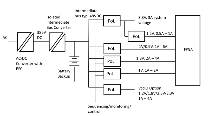
The power distribution schemes used in data centers have also evolved to increase efficiency (Figure 2). ‘Intermediate buses’ generated by AC-DC converters are used to route power at higher voltage, typically 385VDC, which could then be isolated and down-converted to 48V with battery back-up for more local distribution, followed by on-board isolated or non-isolated ‘point of load’ converters for the final conversion stage.
Click image to enlarge
Figure 2: A data center distributed power arrangement
High-efficiency power conversion topologies
Modern high-efficiency conversion topologies all fall into the basic categories of ‘buck’ or ‘boost’ derived, or equivalent isolated versions ‘forward’ and ‘flyback’. All can operate in ‘hard’ or ‘soft’ (resonant) switching modes and feature a minimum of one switch and rectifier, or up to tens of each for the most complex multi-level circuits.
Conduction losses are simply minimized by utilizing switches with lower on-resistances and replacing diodes with synchronous rectifiers, typically implemented with MOSFETs. By paralleling parts, in theory, conduction losses can be arbitrarily low. Switching losses caused by voltage/current overlap, diode reverse recovery energy and charge/discharge of device capacitances are more difficult to control and increase proportionally with frequency. This can frustrate use of Si-MOSFETs at very high frequencies where significant reduction in magnetics size is targeted. Operation in a resonant mode is a solution for some topologies with ‘zero voltage switching’ (ZVS) or ‘zero current switching’ (ZCS), but with care to ensure that damaging, high dissipation ‘hard’ switching does not occur under transient or overload conditions. In this case wide band-gap devices provide some safety margin with their anyway-lower dynamic losses compared with silicon.
Some conversion stages practically must be ‘hard switched’, such as the TTPFC already mentioned, which operates in ‘continuous conduction’ mode at high power to keep peak currents and component stresses within reasonable limits. In this case, wide band-gap devices are invaluable.
The LLC converter - an example of a high-efficiency topology
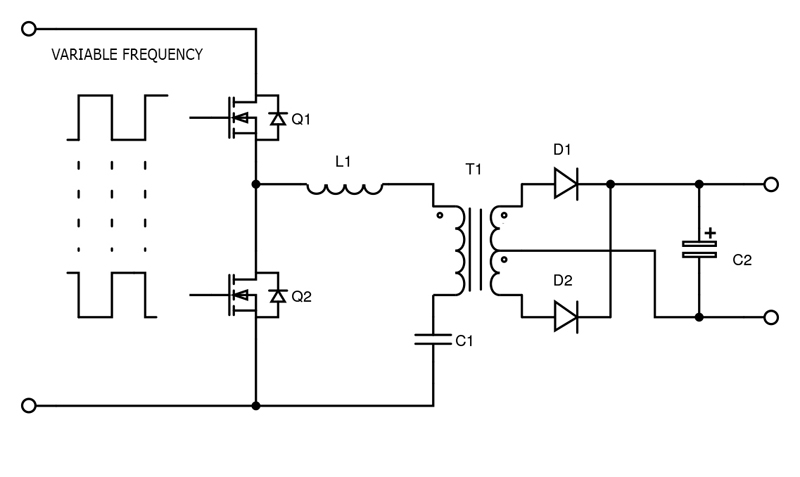
The LLC converter (Figure 3) is a good illustration of a high-efficiency converter. The ‘LLC’ comes from the two inductors and capacitor present in the primary forming a resonant ‘tank’.
Click image to enlarge
Figure 3: LLC converter outline
L1 is either discrete or controlled leakage inductance in the transformer T1 and the second inductor is the primary of T1. Q1 and Q2 are driven at 50% duty cycle in antiphase, at variable frequency and provide a square wave drive to the tank. At the tank’s resonant frequency, its impedance is minimum, and maximum energy passes to the output through transformer action. Away from resonance, the impedance is greater, either inductive or capacitive, and less energy transfers. For a constant output load, this effectively means output voltage can be controlled by varying the drive frequency. Practically, the nominal frequency is set higher than resonance, with the tank looking ‘inductive’ so that zero voltage switching naturally occurs for both Q1 and Q2, for low losses. The transformer primary and secondary current is sinusoidal, so the output diodes see zero-current switching. The LLC is complex to control with multiple resonances occurring, but can operate at very high efficiency.
Losses characterized
It can be hard to judge which switch technology is best for a given topology, frequency and load range so ‘figures of merit’ (FOMs) can be useful. One is RDS(ON).A, the product of device on-resistance and die area. This gives a useful indication of conduction losses for a given die size – it is always possible to reduce on-resistance with a larger die but capacitances and switching losses then increase, along with cost and a decrease in yield per wafer. FOM RDS(ON).EOSS is another measure which combines conduction loss and switching losses from stored energy in device output capacitance, important in ‘hard’ switching topologies. EOSS can be high and variable in Si-MOSFETs, whereas SiC MOSFETs are lower and the value for SiC FET cascodes lower still, for the same on-resistance and device voltage class. The SiC FET is a cascode arrangement of a SiC JFET and a Si-MOSFET. Another parameter which is important is the reverse recovery energy of any body diode effect in a switch, which causes significant dissipation under hard switching conditions. SiC MOSFETs have some low value, but with gains offset by the high forward voltage drop of the diode causing increased dissipation if it conducts in switching ‘dead’ times by ‘commutation’. SiC FET cascodes by comparison have even lower diode recovery energy and much lower forward drop. GaN devices have no recovery effect and conduct in reverse through their channel, but the voltage drop can be high in commutation conditions and is dependent on gate drive voltage levels.
The effect of channel and reverse conduction losses across different switch types can be characterized by the FOM RDS(ON). Qrr and an indicator of performance in high-frequency soft switching topologies is FOM RDS(ON).COSS(tr)where (tr) is ‘time related’.
Switch technologies compared
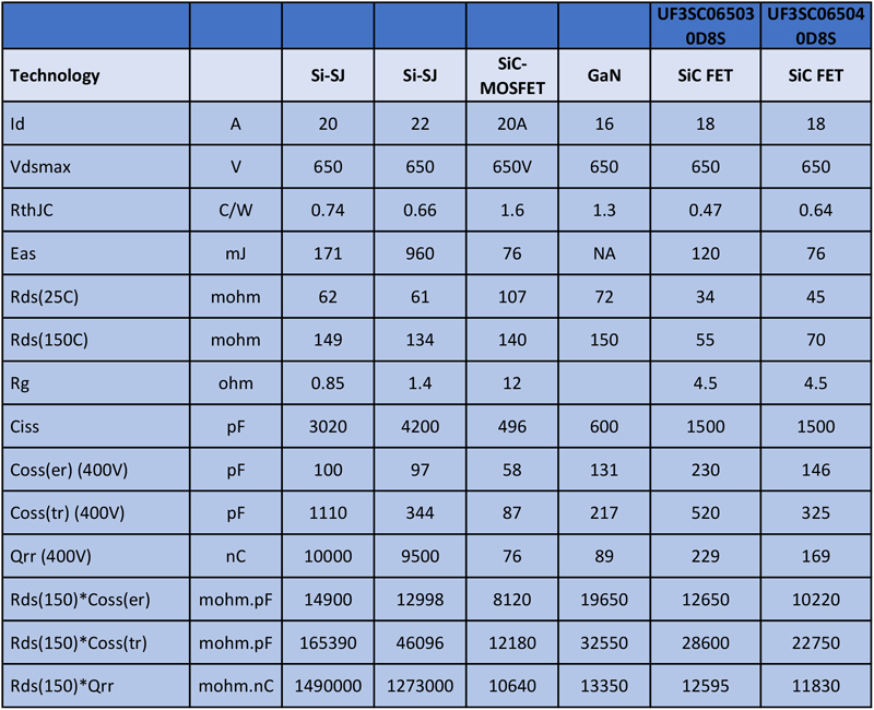
For high efficiency converters, silicon super-junction MOSFETs, SiC MOSFETs, GaN HEMT cells and SiC FET cascodes have been mentioned. A summary of how FOMs compare is given in Table 1 for the same voltage and current class of devices.
Click image to enlarge
Table 1: Comparison of switch characteristics in the 650V/20A class
Advantages of SiC MOSFETs and GaN over silicon for losses can be seen from the table, although avalanche energy rating and thermal resistance to case is worse in the examples shown. However, the SiC FETs shown from UnitedSiC have better or equivalent FOMs, significantly lower on-resistance in the class described and much better thermal resistance to case, achieved with their silver-sinter die attach and wafer-thinning technology.
An additional advantage of SiC FETs is their easy gate drive compared with the other wide band-gap technologies. SiC MOSFETs need a gate drive of around 18V for full enhancement, very close to the absolute maximum, and the gate threshold is variable, subject to hysteresis and affects short circuit withstand. GaN has a low gate threshold voltage, with a similarly low absolute maximum, so must be driven with care to avoid voltage overstress from transients and overshoot, which are real dangers with the high dV/d and di/dt waveforms present.
SiC FETs in comparison can be driven with a standard silicon MOSFET or IGBT gate drive at typically 0-12V, with wide margin to the absolute +/- maximum. The threshold is stable, shows no hysteresis and gate voltage does not affect the inherent SiC FET short circuit withstand rating.
UnitedSiC ‘Generation 4’ SiC FETs now switch so fast that this can be a practical issue when edge rates need to be controlled for minimum overshoots and EMI. The company has shown however that simple low-dissipation snubbers are an effective solution. A new development is SiC FET cascodes with uncommitted JFET gates which allow much better control of switching speed, while the co-packaged cascode Si-MOSFET still allows normally-off operation at start-up, shut-down and under fault conditions.
Conclusion
Wide band-gap semiconductor technology has opened up new possibilities for yet-higher efficiency in power conversion. SiC FETs from UnitedSiC are at the forefront, with figures of merit that excel across the board.