The logical choice for embedded applications
The accuracy of the wafer coupled with assembly processes already commonly found in the manufacturing plants of IGBT modules, makes the chip form of NTC the ideal component for embedding into power electronic modules. The need for thermal management in today's semiconductor devices, such as IGBTs or LEDs, is well documented in the internet. Not so much is how this should be achieved. Thermistor based Sensors Thermistors (temperature dependent resistors) are ideal components for the measurement of temperature. Available with Positive Temperature Coefficients (PTCs) with a resistance that increases with rising temperature and Negative Temperature Coefficient (NTCs) that feature a declining resistance with increasing temperature, thermistors can be found in many electronic systems for temperature sensing and over-temperature protection. Conventional NTCs are either in EIA SMD sizes (0402, 0603, 0805 etc) or leaded and are designed for PCB mounting. Some probes are available for mounting on heat-sinks but these, due to their application, tend to be large robust and hermetically sealed packages which limit their deployment in the majority of embedded semi-conductor not only due to their size but also to the problems of termination. However, due to their compact nature SMD technology is widely used for embedded applications within semi-conductor modules despite that fact that there are a number of difficulties that must be overcome in the module assembly process. These problems can be summarised as follows: 1. The terminations must be located on the substrate in the form of pads (either for soldering or for gluing) 2. The part is generally delivered on tape or in a cassette 3. The surface of the actual NTC is not always in contact with the substrate to which it is attached 4. The differing temperature coefficients between the NTC material and the substrate can lead to cracks 5. The over-moulding process can also place additional mechanical stresses on the body but also the terminations which can also lead to cracks in the ceramic
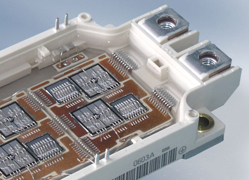
Whereas the majority of these issues can be overcome with the necessary investment in processes and machinery, the problem with cracking, (Fig.1) which is mostly due to the soldering and assembly process, is not so easily solved. Even if the process can be optimised during the assembly process (control of the placement pressure, centralising of pick and place head etc), the problem of the potential forming of cracks due to the temperature cycling of the NTC through the semiconductor itself during the lifetime of the product itself will always remain unsolved and overtime can therefore still become a quality issue. The solution here is to use an assembly process that is already widely used within the semi-conductor manufacturing industry itself: NTC Chips TDK-EPC has used a wafer based technology for many years in its manufacturing process of so-called mini-sensors (Fig.2). The advantage of this technology versus the deployment of a SMD device or disc is that the dicing process is physically linked to the electrical properties of the complete wafer (Fig.3). Hence the dicing process, in combination with appropriate trimming for the finished chip, can be realised with extremely tight tolerances.
An additional advantage of the wafer technology for chip NTCs solves the problem of the electrical connection. As the terminations are no longer on the component edges (as with a SMD) but on the top and bottom surfaces (Fig. 4) direct contacting to the module substrate on one side and wire bonding for the second connection are now possible. Hence the solder process can also be eliminated.
However, the major advantage that is especially beneficial for the semi-conductor industry, is that the temperature for this measurement process and hence the subsequent dicing can be undertaken at higher temperatures - typically 100°C.
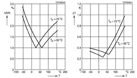
Through this, the inaccuracies of the NTC R/T characteristics can be for the most part eliminated and as a result the IGBT can be safely operated much closer to its' maximum junction temperature limits. The reason for this better measurement control can be explained as follows: The difference in tolerance between a rated resistance at 25°C and 60°C can be expressed in D resistance (Fig.5) and in D temperature (Fig.6). The maximum accuracy is hereby achieved at the rated temperature.
Through this, the inaccuracies of the NTC R/T characteristics can be for the most part eliminated and as a result the IGBT can be safely operated much closer to its' maximum junction temperature limits. The reason for this better measurement control can be explained as follows: The difference in tolerance between a rated resistance at 25°C and 60°C can be expressed in D resistance (Fig.5) and in D temperature (Fig.6). The maximum accuracy is hereby achieved at the rated temperature.
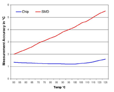
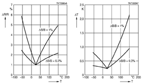
However in addition to the resistance tolerance, the accuracy of the B-Value should not be ignored since also defines the precision of the temperature measurement. By definition a lower B-Value tolerance results in a more accurate result (Figs.7 and 8). The net result of these critical parameters can be seen in the change of resistance over temperature between a Chip rated at 100°C and a SMD rated at 25°C (Fig. 9). With a change in resistance of up to � 5°C at 115°C for the 0603 SMD (3% B tolerance; 5% R25 tolerance) the microcontroller will need to reduce the power of the IGBTs at 120°C to ensure that the junction temperature does not exceed 125°C whereas due to the inaccuracy of the NTC the actual junction temperature may only be 115 °C. The wafer rated at 100°C (1% tolerance, 3,5% R100 tolerance) would have a temperature inaccuracy of only � 1.5°C at 120°C meaning that power derating is only necessary at 123°C to ensure a safe junction temperature assuming 125°C is its' limit. It should also be pointed out that with the SMD these conditions only apply to the delivered state, an additional drift of up to 3% needs to be considered after the soldering process. An additional advantage of this technology is that the maximum operating temperature is 155°C and this depending on IGBT requirement could be increased to 175°C and the B-Value tolerance could be further tightened to 0.5%. Terminations The terminations of the chip surface can be adapted to the mating surfaces with a silver electrode or gold if this is more desirable for the wire bonding process. Certification Recognition by Underwriters Laboratories according to UL 1434 has already been secured. Summary Hence the accuracy of the wafer coupled with assembly processes already commonly found in the manufacturing plants of IGBT modules, makes the chip form of NTC the ideal component for embedding into power electronic modules. For more information on these devices and their application please contact: design-solutions@epcos.com www.epcos.com


