Isolating SPI clock, control, and data lines aids link robustness but requires timing and data-rate analysis.
The simple SPI (Serial Peripheral Interface) bus is a popular serial interface commonly employed in automotive, industrial-control, and communication applications. To provide isolation and minimize the effect of ground loops, optocouplers are de-facto standard in these systems. They ensure data integrity and provide electrical safety in noisy and hazardous environments. However, adding optocouplers to the serial-data channel affects the data throughput. The SPI protocol bit timing depends on the data bit rate and optocoupler propagation-delay time.
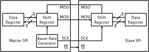
The SPI bus provides a four-wire synchronous serial communication interface, often between an MCU and peripheral devices. The four wires are MISO (Master Input / Slave Output), MOSI (Master Output / Slave Input), SCK (Serial Clock), and SS (Slave Select or Chip Select). The main control element of an SPI subsystem is the SPI Data Register. There are two 8-bit data registers: one in the master and one in the slave. Together they form a 16-bit register linked by MISO and MOSI pins (Figure 1). Only a master SPI module can initiate data transmission. A transmission begins by the host processor writing to the master data register. If the shift register is empty, the byte immediately transfers to the shift register and then shifts out on the MOSI pin under the serial clock's control. Only the master SPI module generates the serial clock signal and synchronizes data communication with slave devices. A master SPI module usually configures the SS pin as a Slave Select output. Before data transmission occurs, the SS pin must assert low and remain low until the transmission is complete. Allowing SS to go high forces the SPI port into its idle state. There are two types of SPI connections that include one master and multiple slaves: daisy-chain cascaded slave devices and parallel-linked slave devices. The slave device could also work with several masters via the multi-master protocol. Here, we focus only on the single master/slave connection because the timing sequence for multiple slave devices is similar to the timing for a single-slave connection.
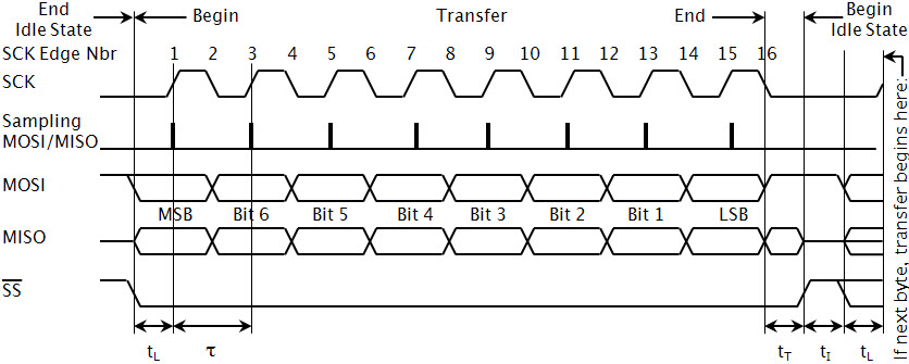
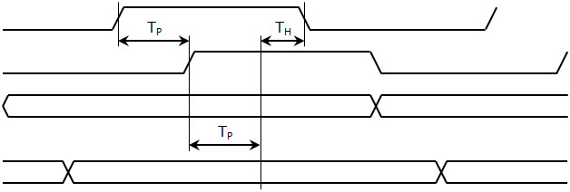
Sometimes the SPI port communicates using only three wires. This is possible when a peripheral device is in a fixed configuration and only sends out data, eliminating the need for an input signal. Similarly, or if the peripheral only inputs data then the bus can operate without the output signal. The SPI timing chart illustrates the control settings for the SPI port (Figure 2): Clock active-high (CPOL=0), data sampling occurs at the clock's odd edges (CPHA=0), data transfers MSB first (LSBFE=0). A write or read to the master's data register initializes the data-transmission operation. In typical SPI data transmissions, the first clock edge issues a half cycle after SS goes low. The first edge on the SCK wire clocks the first data bit of the master shift register into the slave via MOSI and at the same time, the first data bit from the slave clocks into the master via MISO.
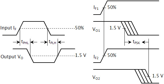
When the subsequent second edge on the SCK wire occurs, the previously latched data shifts into the shift register's MSB (most-significant bit). The same operation repeats through to the 16th edge of SCK at which point all eight data bits from the master have shifted into the slave and all eight data bits from the slave have shifted into the master. After the last bit shifts in, data are transferred into the parallel SPI data register from the shift register. From the last clock edge, there is a minimum of a half clock cycle trailing time, tT, before the clock level goes high and SPI begins next idle state. The SS wire retains the high state for a minimum half clock cycle idling time, tI, before the clock level goes low again. Timing and data-rate calculation Before inserting optocouplers into the SPI interface, let's analyze the relationship between the optocoupler's propagation-delay time and the signal data rate as it passes through the optocouplers. An optocoupler's maximum high-to-low and low-to-high propagation delay, (tPHL and tPLH), will indicate the device's maximum data transmission rate (Figure 3). The maximum propagation delay tP(MAX) is the greater of tPHL or tPLH. An optocoupler transmitting NRZ (non-return-to-zero) data requires that the data bit period, ?, is at least greater than tP(MAX) :

So, the maximum data rate is:

For a clock signal that employs RZ (return-to-zero) coded data, a clock cycle includes both the high and low period: ? = tHIGH + tLOW. For an optocoupler to transmit a 50% duty cycle clock signal requires that half a clock cycle be greater than tP(MAX):

and the maximum clock frequency is:

When data transmits synchronously over parallel signal lines, the optocoupler's propagation delay skew, tPSK, is an important factor that may determine the maximum parallel data transmission rate. If the parallel data transmits through two individual optocouplers or one multi-channel optocoupler, differences in the propagation delays between channels will cause the data to arrive at the optocouplers' outputs at different times—the skew. If this difference in propagation delay is sufficiently large, it will limit the maximum rate at which parallel data can transmit through the optocouplers. Propagation-delay skew is the difference between the minimum and maximum propagation delays of tPLH and tPHL for any group of optocoupler channels operating under the same conditions of drive current, supply voltage, output load, and operating temperature (Figure 3). The optocouplers' tPSK will result in uncertainty in both data and signal lines. In general, the absolute minimum pulse width that can pass through parallel optocouplers is twice tPSK:

The maximum data rate is, then:

A conservative design should use a slightly longer pulse width to ensure that any additional uncertainties elsewhere in the circuit do not cause problems.
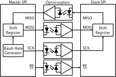
Figure 4 shows a typical 4-wire SPI isolated interface, with each MISO or MOSI wire employing one channel or one optocoupler to provide the electrical isolation between the master and the slave. This example will calculate the isolated-interface timing and data-rate using multiple Avago ACPL-M72T optocouplers to provide the isolation on the signal wires (MISO, MOSI, and SCK). From the optocoupler's data sheet, the tP(MAX) is 100 ns and tPSK(MAX) is 60 ns. Substituting those values into the previous equations, we can determine the maximum SPI data rate. Because the SPI clock is a return-to-zero signal, first apply eq 2 to the SCK signal and calculate the maximum clock frequency:

Because the master device sends out the MOSI and SCK signals in parallel and synchronously, next apply eq 3 on the two wires to determine the maximum data rate on MOSI due to potential signal skew:

The synchronization of the MISO and clock signals is different with MOSI. When the clock signal is transmitted from the master to the slave, the optocoupler contributes propagation delay skew once on SCK. After slave receives the clock signal, the slave outputs data to the master, and the optocoupler in that path contributes its propagation delay skew on MISO. The master must sample this data before the same clock signal's second edge transition. Thus, two times the propagation delay time should be less than half of the clock period: 2tP(MAX) ? ?/2 and, therefore, the maximum data rate on MISO is:

Finally, once the lowest data rate is determined, that rate should apply to all calculations. Comparing the three data rates of fSCK, DRMOSI and DRMISO, the lowest data rate is DRMISO at 2.5 MBd, and the corresponding clock frequency should be set to 2.5 MHz, which is the safe limit to transmit data without any missing bits. A slightly more conservative approach would set and even lower clock frequency of about 2 MHz rather than calculated 2.5 MHz, to ensure data integrity for any additional uncertainties.

The SS wire usually has a longer idling time, tI, between data transfers and can thus use a lower-speed optocoupler. Table 1 lists various SPI clock frequencies, the maximum data rates, and the maximum propagation delays required for the optocouplers. Avago Technologies
- SPI block guide V03.06, Motorola, 2003.
- Junhua, He, Assuring data integrity in an optically-isolated 3.3 V I2C bus, White paper AV02-2384EN, Avago Technologies, 2010.
- Junhua, He, Digital optocouplers deliver low power consumption and high isolation for automotive applications, White paper AV02-3220EN, Avago Technologies, 2011.
- ACPL-M72T High-Speed Low-Power Digital Optocouplers, Data sheet AV02-2180EN, Avago Technologies, 2011.


