Accurate primary-side-sensing controller
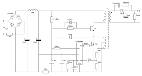
The universal drive to reduce power consumption that Energy Star and similar initiatives have so successfully promoted within consumer-level equipment is starting to take a real hold within industrial systems, and embedded controllers and their peripherals in particular. Applications as diverse as fire alarms, process controls, and building automation systems very often operate on low duty cycles that potentially waste significant amounts of power while they await the next cycle of computation and communications activities. As a result, designers are under pressure to develop systems that intelligently power down whenever it is practical to do so, and run as efficiently as possible under the expected set of active-mode conditions. These considerations demand power supplies that offer very low standby power consumption together with the ability to quickly return to full output power while maintaining accurate regulation. Naturally, any power supply solution must also offer a raft of complementary benefits —such as excellent electrical performance, robust fault protection, and minimal EMC issues — at the lowest cost that is consistent with reliable design. CamSemi's recently-introduced C2163 is a universal-input, primary-side-sensing control IC that meets these criteria while offering a range of output voltages at power levels from about 8W to 18W to suit a wide variety of embedded applications. An evolution of the C2161/62 family that suits applications of up to 8W, the C2163 substitutes an output stage that is tailored for driving the gate of a MOSFET in place of the bipolar-transistor emitter driver that appears in the original devices. This conceptually simple change allows the new six-pin SOT-23 packaged device to control substantially more power at minimal additional component count and cost while retaining all of the benefits that the original parts deliver—see Figure 1.
Operating principles The C2163's operating principles are easily understood by considering figure 1. The general circuit arrangement echoes a conventional flyback converter that includes an auxiliary power winding to supply the controller chip and an additional winding that provides a feedback sense voltage. All power conversion occurs in discontinuous conduction mode, with the C2163 varying its switching frequency and on-time in response to load demands. The device switches the main primary winding via Q1 and Qe, where Q1 is a high-voltage bipolar power transistor (700V blocking for universal-input designs) and Qe is a low-voltage logic-level MOSFET. This cascode-connected pairing is cheaper and typically more efficient than a single high-voltage MOSFET, and it benefits from quasi-resonant switching that turns the devices on when feedback detects that the voltage across primary switch Q1 is at its minimum. Together with a degree of natural frequency jitter that spreads emissions, this "soft" switching technique eases EMI concerns to minimise the need for conducted-emissions filtering. At power-on, current flows from the high-voltage dc input rail via the high-tension resistors Rht to supply the C2163, which enters its initialisation mode. The controller then issues several clock cycles that switch the main primary winding via Q1/Qe. This induces a potential in the auxiliary winding and operating current starts to flow via rectifier Daux. An internal shunt voltage regulator stabilises the chip's supply and the device enters run mode, with feedback being applied via scaling resistors Rfb1 and Rfb2 and coupling capacitor Cfb. The network Rosc and Cosc sets the maximum oscillation frequency, which lies between 40kHz and 66kHz at full load. The value of Cosc also determines the C2163's integral cable compensation level that automatically allows for a variety of PSU to load cable, track, or output filter inductor resistances, with a 1% minimum being set by design. Resistor Rcs sets the range of pulse-by-pulse current control and the nominal overcurrent point. Inspection reveals that the voltage developed at the chip's CS current-sense pin is negative with respect to chip ground, which is intentional if unusual. The output range that this basic circuit offers, spans voltage levels from 3 - 24VDC and 0.5 - 5A at power levels of up to about 18W. It betters the operating efficiency requirements of Energy Star EPS 2.0 — and its recent embodiment within IEMP Level V — with at least 2% margin and has a no-load power level below 100mW, which is a factor of three times lower than this benchmark specification requires. Importantly, a few minor circuit modifications can improve upon output power levels and drive down no-load power consumption to make the topology's application potential significantly more flexible, enabling cost reductions by amortizing design effort and rationalizing inventory holdings. Smart sensing improves performance, lowers cost This implementation of a flyback topology embodies multiple features that help optimise its performance while minimising build cost. For instance, a voltage reference with optocoupler feedback is traditionally necessary to meet the 5% or better regulation that commodity ICs require; without this correction, a typical primary-side-sensing controller exhibits considerable load-current dependency and may manage only �10 to 15% regulation accuracy. By contrast, the C2163 easily betters �5% using a proprietary mixed-signal technique that allows the chip to precisely determine the amount of energy that is necessary to maintain regulation over the circuit's operational range (in practice, �2% is achievable given minimal load-resistance compensation). The chip is also capable of maintaining �7% current regulation if the application requires constant-current mode operation. This feature can also be used as a load current limit for constant voltage applications, protecting the PSU and load under fault conditions. Significantly for many industrial applications, the circuit topology is highly resistant to single-fault conditions and will protect the load by entering "hiccup" mode if the chip senses inappropriate external conditions. This action limits output voltage and current in the event of a single component failure
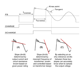
The key to the C2163's regulation performance lies with the controller's ability to examine the tangent of the slope to find the knee point during the energy transfer phase, as figure 2 shows. At the knee point the secondary winding current has fallen to zero, so resistive volt drop is also zero, allowing accurate voltage sampling. The circuit's output current and circuit resistance are known by design and set the initial dV/dT slope, as in (A). Similarly, the second slope (B) is known as a function of the transformer's resonant frequency, which is again fixed by design. An on-chip reference dV/dT slope (C) then makes it possible to assess precisely when to sample the output voltage. The ac coupling that Cfb provides allows the chip to sample the entire waveform, rather than just finding the knee point and zero-crossing points. This allows the chip to implement mains under-voltage lockout, mains over-voltage protection, and to protect the power transistor during de-saturation. Other refinements include leading-edge suppression to quash the transient that appears in the current-sense waveform at the start of the charge phase that may otherwise corrupt the chip's primary current measurement. Lowering no-load power consumption Dispensing with the need for optocoupler-style feedback or linear post regulators not only saves space and cost, but also improves reliability while reducing power consumption that is especially significant for no-load measurement conditions. Clearly, industrial applications are unlikely to reduce standby current consumption to no-load levels, yet the no-load condition remains a useful benchmark for power-supply designers. In particular, the ability of a controller to recover from a no-load to full load current step is an extreme test of the circuit's dynamics, and designers can expect significantly better performance when switching from light standby-level loads to normal operating currents. The basic circuit in figure 1 achieves a no-load metric of <100mW by minimising the PWM waveform's on time and frequency during light load conditions, but primary-side sensing makes it necessary to pulse the output periodically in order to acquire feedback information. There is inevitably a balance to strike between the frequency and duration of these "radar echo" pulses, the speed of response to an instantaneous rise in output current demand, and power consumption. The tangent detection technique contributes here too as it allows the controller to minimise the turn-on period during unloaded operation. For application designers, response to a low power to normal load current step becomes a function of the resistance of the output interconnection system, the amount of hold-up capacitance present on the output, and the recovery characteristics of the controller's internal loop. This last term depends upon the C2163's minimum no-load frequency, which is set by components within the chip's power supply network — the controller has no intrinsic minimum operating frequency.
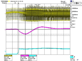
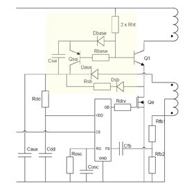
Figure 3 shows a representative 50mA to 1A load recovery sequence where the blue trace is the load step, the yellow trace is the controller's switching waveform, and the purple trace is the output rail. These plots are from a 12V 1A universal-input design. A few additional components can reduce the <100mW no-load power consumption that figure 1 achieves to typically 50 - 60mW, as the "super-bootstrap" circuit (patent pending) in figure 4 outlines. Here, the value of Rht is about ten times that found in figure 1, but the current that it provides to Q1's base is amplified with the resulting emitter current charging Caux and Cdd via Dsb and Rsb. This technique significantly reduces the static power dissipation of Rht and hence no-load power consumption. Once the circuit commences switching, the voltage level on Caux due to the charge from the auxiliary winding keeps Dsb reverse biased and prevents any further Rht-induced Q1 current flow to Caux.
Output power considerations Assuming appropriate support components, the circuit's maximum power output primarily depends on the amount of current that Q1/Qe can handle. In practice, this holds true up to about 18W as a result of the C2163's operating characteristics. For levels of up to about 12W that involve peak switching currents of some 1.5A, the FJE3303 is preferred for Q1 while Qe can be virtually any 20V or better rated MOSFET that has logic-level drive compatibility and RDSon of 0.5? or less. As output power levels rise to 30W, the power switches must handle peak currents of around 4A and an RDSon value of around 0.070? becomes necessary to minimise losses. The recommended bipolar transistor is now an MJE13005G and designers need to ensure that voltages around the part do not exceed its reverse-bias safe-area-of-operation envelope. This consideration typically demands a simple snubber network across the transformer's primary winding. As every power-supply designer knows, meeting EMC requirements often requires multiple iterations of circuit layout and filter-component selection. Following conventional practice, keeping layout tight around the C2163 minimizes loops that contribute towards radiated emissions while the chip's soft-switching and frequency jitter particularly helps to lower conducted emissions and reduce the values of filter-network components. As always, filter-circuit selection depends on output power level, with a single inductor Lfilt of 330μH between Cin1 and Cin2 of equal 15μF values being the starting point for the 12W design in figure 1. Other components that contribute to constraining EMI include the MOSFET's gate-drive resistor Rdrv and the output-rectifier snubber network, Cssnub and Rssnub. Transformer construction is important too, with the C2163 allowing several possibilities to achieve the best balance between ease-of-construction and electrical performance. To assist designers, CamSemi offers extensive application support that includes reference designs and evaluation boards for 12W and 18W supplies. www.camsemi.com


