Optimizing output noise through low-noise power design
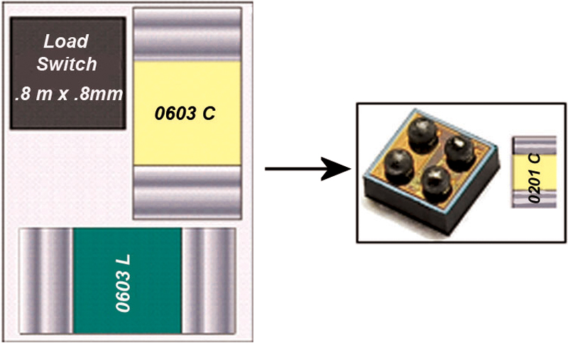
Figure 1: Micrel's MIC94300 integrated design reduces the combined footprint of filter and load switch by as much as 65%.
The proliferation of portable connectivity devices over the last decade has seen most of us become more reliant on technology than ever before. At home and at work, as we embrace technology, we demand convenience, ease of use, and optimized reliability and performance. These demands, allied to increasingly compressed design cycles, present challenges for design engineers, one of the most significant being the issue of the noise performance of power supply rails and the adverse effect that this can have on end-device functionality. Here, we examine the issue of signal noise, and a novel platform that addresses the issue in a single form factor. We will also explain how this same technology can apply to an LDO (low dropout) linear regulator to achieve unmatched PSRR (power-supply-rejection ratio) performance from DC to 10 MHz. Incumbent issues Traditional power components, for example, the DC-DC converters used in high-performance consumer devices such as GPSs, mobile phones, and image sensors, in many cases no longer offer the performance levels that their applications require. As the microelectronics industry continues to evolve, new generations of devices will require extremely low-noise power-supply lines, especially within RF sections. This is vital for the effective and reliable performance of these devices and for avoiding annoying breaks, malfunctions, and service drops due to a poorly performing power converter. In GPS applications, for example, the receiver is highly sensitive and may need to decode very low-power signals on the order of ?160 dBW. Power-supply noise increases the GPS signal acquisition time and reduces position accuracy, which can have an obvious affect on performance. In mobile phones, supply noise can cause dropped calls and reduce signal strength, problems consumers are no longer willing to tolerate in a highly competitive market. Image sensors also benefit from a clean power supply with greatly improved signal-to-noise ratio delivering higher image quality. In these noise-sensitive systems, additional power supply filtering is a vital engineering consideration to meet these most stringent design requirements. Camera modules and image sensors require very wide dynamic range, operating from daylight to nighttime conditions. Low power-supply noise and ripple help to improve this. To achieve the desired cleanliness of power lines, conventional wisdom dictated filtering implementation by simple LC filters in the supply lines. The purpose of these filters is to reduce the switching regulator's ripple voltage. With skilled circuit design and PCB layout, the output ripple of a buck regulator is typically one percent of the output voltage. For example, one could reasonably expect a 2.5-V output to produce about 25 mV of output ripple. The LC filter attenuates the switching regulator's output ripple. A simple output filter can reduce this noise by anywhere from 20 to 40 db—factors of 10 to 100—and any high frequency spikes which may be superimposed on the ripple are attenuated by even more (reference 1). This incumbent method is not perfect and presents challenges to designers in environments where PCB real estate comes at a premium, adding pressure to reduce component footprint as much as possible while maintaining desired performance. Optimizing noise attenuation To address the ongoing issue of output ripple, significant work has taken place to develop means of noise attenuation while offering significantly more stable performance in a reduced footprint. Goals include a low cut-off frequency to achieve sufficient suppression and noise reduction on critical supply rails with a single pole LC filter, which to this point has meant using a multitude of space and cost-consuming LC filters. In portable applications, a semiconductor switch is also required to save power, a factor that previously increased the required PCB board area. An example of single-chip device that combines both the filter and switch is the MIC94300, which Micrel calls the Ripple Blocker. This active filter provides high-frequency ripple attenuation and switching noise rejection. Comprising an active filter integrated into an LDO linear regulator and load switch, this topology makes a significant difference in numerous high-volume consumer products such as mobile and smart phones and tablets in terms of enhancing performance and sustaining connectivity integrity. The main advantages of designing active, rather than passive, filters into power supplies are threefold. Firstly, the integration of the active filter in the silicon offers significant savings in terms of component count and PCB real estate. In this case, the single-chip design reduces the PCB footprint by as much as 65% (figure 1). Active filters also provide the capability to implement multiple order filters or achieve a certain filter passband shape or lower corner frequency virtually independent of package size.
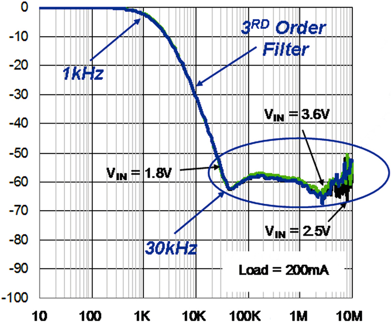
Another advantage active filters have over LCs is their superior transient response and avoidance of the ringing effect LC filters often experienced. This puts less demand on load circuits' PSR (power supply rejection) and reduces cross coupling to sensitive adjacent nodes. An active-high enable pin controls the MIC94300's load switch. Forcing the enable pin low turns off the load switch, setting it to a near-zero off-mode current state. When enabled, the load switch is biased near its saturation region to maintain optimum performance between low RDS(ON) and ripple rejection. The result is roughly a 170-mV fixed voltage drop between the input and output voltages. The IC protects itself from damage due to fault conditions, offering linear current limiting and thermal shutdown. The device achieves a supply-noise attenuation of about 60 db—a factor of 1000—from 30 kHz to 10 MHz, constituting a tenfold improvement over the LC filter at a switching frequency of 300 kHz (figure 2). The internal active filter passes DC and blocks any AC components with a frequency beyond 1 kHz. A third-order filter provides a steep roll-off so that most of the attenuation is available from 30 kHz to 10MHz. This means that, for the designer, virtually all switching-regulator output-ripple components will reduce by about 60 dB, which is a vast improvement in design margin in any portable design compared to incumbent technologies. The IC maintains its low 170-mV drop over varying loads, optimizing power efficiency. Most available LDOs will not produce this level of PSRR for such a small voltage drop over such wide bandwidth while consuming just 140 μA of ground current. Applications in capacitive touch sensing using this method as a very low-noise and -ripple power source benefit from improved sensor accuracy, and there are a wide range of emerging applications that will use capacitive-sensing technology, including smart phones and tablets. Motor applications using Hall Effect devices detect the rotation angle of small brushless DC motors. Eliminating noise at the power source of the Hall Effect device improves the Hall sensors' precise signal response over operating range and the performance of the motor.
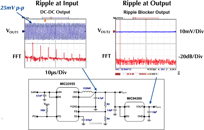
A typical application illustrated An example of a typical application circuit includes an MIC23155 synchronous-buck switching regulator and an MIC94300 (figure 3). The buck regulator steps down the 5-V input to 2.5 V. The regulator's switching action creates the output ripple that appears on the output capacitor. The magnitude of the output-voltage ripple depends upon the inductor ripple current, the output capacitance value, its ESR (effective series resistance), and its ESL (effective series inductance). The circuit achieves a 25-mV peak-to-peak ripple across the output capacitor. The fundamental frequency of 314 kHz is the switching frequency of the buck regulator, with harmonics being multiples of the switching frequency. The MIC94300 provides a more than 40 dB improvement in rail noise over the spectrum of interest. The ripple at the output is near to zero with switching harmonics virtually eliminated, as the low RDS(ON) of a current limit switch combines with the PSRR capability of an LDO. First, the LDO maintains a fixed voltage drop of 170mV that is independent of load current. An internal 170mV referenced to the input voltage sets the voltage drop. A low-pass filter passes the DC and blocks the AC component of the input voltage. The filtered signal serves as a reference to the LDO so the output will follow the DC of the input but rejects any AC signal. The use of an NMOS pass device provides an extremely low dropout as used in current limit switches. This technology can also apply to LDOs to produce fixed output voltage with high PSRR from DC to 10MHz. Here the device regulates the output voltage like a basic LDO regulator, where a resistor-divider network connecting the output and ground sets the output voltage. Standard P-channel LDOs have high PSRR at DC but start losing ripple rejection typically above 10 kHz. This roll-off is due to the gain-bandwidth limit of the error amplifier. The MIC94310 does not have this limitation because it uses an NMOS pass device configured as a source follower and has intrinsically good PSRR due to its low output impedance. This means that a smaller loop gain is necessary to achieve the same PSRR as when using a PMOS as a pass device. Therefore, at higher frequencies where the loop gain drops, an NMOS pass device can still maintain a good PSRR. The MIC94310 surpasses the performance of a standard LDO at frequencies from 1 kHz to 10 MHz. This type of product is, therefore, highly suitable for use as a regulator with a switching regulator input voltage whose fundamental switching frequency is typically in the 500 kHz to 3 MHz range. Micrel References: 1. Nelson, Carl, LT1070 Design Manual, Application Note 19, Linear Technology.


