Best practices for reducing power, improving productivity and delivering SoCs on time and on budget
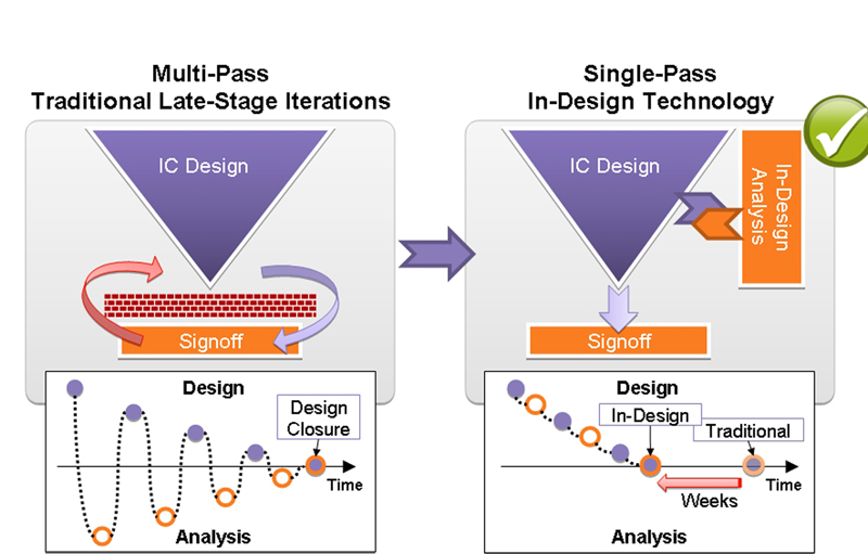
Figure 1: Benefit of In-Design Technology in IC Design
Power has always been an integral part of consumer electronics, but increasingly we can do more things with a single device. That trend, above all others, has moved power consumption from an afterthought to a critical part of the architecture of the processor, the SoC and even the end device itself. For SoC architects and engineers at all levels of the design flow, the tradeoffs between area, power and performance are now unevenly weighted toward power. And while there are numerous tools on the designer's belt to solve these problems, the burden each of those places on the verification side of the process has become overwhelming. All of this can mount up very fast in terms of cost, both in non-recurring engineering hours and re-spins after initial tapeout, which at advanced nodes can easily run into the tens of millions of dollars. But even those costs pale in comparison to the cost of a missed market window. Architecting a good plan Every SoC requires lots of up-front planning. The better the plan up front, backed up by previous experience, the less pain when it comes to verifying that everything works. Creating a good plan requires a learning curve at 45nm and beyond because there are simply too many gates and wires and too many interactions across multiple power islands to use the old methods of doing things. High-level models need to be created to be able to spot inconsistencies up front, whether that includes high-level synthesis for the RTL, software prototyping models or power modelling in the architecture. At 45nm and beyond, each one of these techniques speeds up the design process. Below 28nm, it's virtually impossible to create a chip in a reasonable market window without them. Using those models, architects need to map the future functionality of an SoC. What is the first chip that will be derived from a model and what will the last derivative look like? Will the functionality be built into software or hardware? Will the intellectual property blocks come from multiple vendors and do those blocks work at the same voltages? Moreover, what are the marketing goals for the chip? What is the minimum performance and the maximum power usage? Will battery life be a competitive issue? How many functions will be combined onto the chip versus another chip in a package? Perhaps even more troublesome is the testing of the IP blocks and the models themselves. From the from the architecture of the block to the environment in which it is used, low power operating modes and conditions are notoriously difficult to reproduce and test. And with packaging now considered an important aspect of the overall design, particularly when it comes to power dissipation, the problem becomes even more complex. In fact, the only place where some of the complexity has been taken out of the design is in the layout. Restrictive design rules imposed by foundries for the majority of their customers at 32nm and 28nm is a way of making sure that when a chip gets designed, it can actually achieve reasonable yields. These are business driven rules so the foundries can successfully build chips. But even in this case, Design Rules Checking complexity is way up, and new problems due to extremely small geometries are being introduced. Design for manufacturing suites can help refine the layout even further and offer a number of tradeoffs in terms of what happens when polygons are drawn one way versus another on a piece of silicon. Increasingly, however, even those tradeoffs are no longer just performance and area-based. The parasitics of the interconnects on a chip have become incredibly complicated. Power, both static and dynamic, needs to be taken into account throughout. So does the ability to manage those tradeoffs. In the past, if this was done at all, it was typically done by hand. There are now tools to make this all work. None of this can be done purely statically anymore. The impact on I/O and timing can be modeled statically, but they need to be tested dynamically—and usually with at least a prototype of the software that will be running on the hardware once it is developed. And if the entire team wants to succeed, they now have to start having conversations up front with the people who will be testing and verifying the entire system. A novel approach to managing the pain in chip design is using "in-design technology," a concept that is fast becoming much more important at advanced technology nodes. Rather than just developing the pieces—circuits, blocks, etc.—through individual steps in the flow, analysis technology is shared at each step. For engineers used to working with individual point tools rather than a suite of tools, this is something of a change. While individual tools can be used, the bigger picture needs to drive them and take priority in order to ensure the best optimization and smooth signoff. That's why it's absolutely vital at the most advanced geometries to use the most integrated tools available at each step of the design process rather than just point tools that do a specific task without understanding the other parts of the process. At advanced nodes the requirement for integration of tools that understand power can mean the difference between hitting a power budget and creating a very costly mistake. Synopsys IC Compiler uses in-design technology to leverage the analysis engines of Primetime® for timing analysis, PrimeRail for power rail analysis, and IC Validator for physical verification during the physical implementation process to identify and avoid potential problems, and accelerate overall time-to-tapeout.
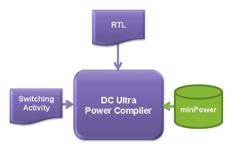
At a much higher level, Synopsys DesignWare® minPower Components allow DC Ultra with Power Compiler™ to use power-costing as the basis for high-level datapath architectural choices. These are examples of integrated technology for power management and optimization within the Galaxy™ Implementation Platform. Similarly, within the Discovery™ Verification Platform, VCS® with MVSIM performs voltage level-aware simulation with an understanding of voltage values to ensure correct operation of complex low-power designs. Getting the team to work together There's a big difference between the way hardware and software engineers approach problems, and that difference is magnified the further up the software stack you move. That means both teams have to work together and be in sync throughout the development of the chip. A change on one side has to be reflected on the other, and it has to be reflected in all the models that have been created, whether they're for power, hardware blocks, transactors or software—including prototypes of software that will run on the hardware. In the power realm, a change in the hardware can affect how efficiently the software utilizes that hardware. The corollary is also true, where a change in software can impact the power efficiency of the hardware. For example, an RTOS that does exactly what a specific size core or processor needs can use significantly less power than a Linux operating system on a general-sized core. Likewise, a powerful multicore processor running a single-threaded software application or kernel is no faster than a single-core processor running the same software. But this kind of synchronizing of hardware and software teams can only be achieved with buy-in from upper management and choosing tools that can work together. Companies that have begun to deploy these kinds of bridges report success in churning out chips at the most advanced process nodes on time and on budget, normally using engineers that can bridge the gap between the hardware and software engineers. They basically work as translators back and forth between the teams as they move down the line toward tapeout. Verifying it all works Final verification of a complex SoC has certainly become a daunting task. But assuming all the necessary steps were taken up front, that pain can be eased substantially. IP can be verified even before it is used in a design. Pre-existing blocks can be verified. And models can be verified in advance. What cannot be fully verified are the interactions between aspects of the chip and all the variables that go along with them. Consider the smartphone example. A person is listening to music when a call comes in. Does the music power down and then power up when the call is finished, or does it remain on in the background? And if it does stay on, how does that affect the thermal budget? With these complexities understood and the right tools and support put in place right from the start, projects with power as a key differentiator, need not be so painful. www.synopsys.com