ISO 11898-compliant HS-CAN communication from a high-speed CAN transceiver supplied by a charge-pump
Charge pumps are often the best choice for powering a CAN-bus application that requires a combination of low-power, low-voltage operation and low cost. This article explains how to supply a high-speed CAN transceiver, via a charge pump, to achieve a 5V rail that is required for most transceivers to deliver ISO 11898-compliant communication in automotive electronic control units (ECUs) that only have a 3.3V supply available. The article also discusses the impact on electromagnetic emissions and immunity.
Over the past several decades the automotive industry witnessed a rising demand for more comfort, efficiency, and environmental cleanliness, and a growing expectation for better performance and safer vehicles. As a result of these trends, the number of electronic subsystems in a car and the wiring to connect all of them was increasing significantly. With more wire, there was more weight to the vehicle and, of course, more cost. However, in the early 1980s Bosch developed the CAN-bus network, which has now been widely adopted by the auto industry since the bus network offers many advantages including reductions in wiring harness complexity, weight, and cost.
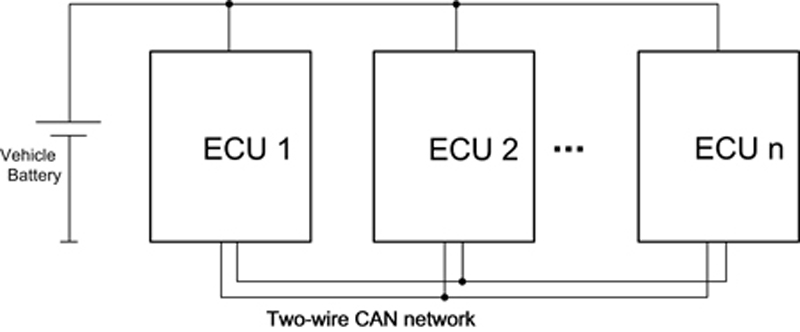
The transition from a centralized control system to distributed systems in automobiles helped the automotive manufacturers meet their goal of reducing the weight and cost of a vehicle. A centralized control system has all actuators, sensors, and switches connected to it through multiple wires. A distributed system locates the electronic control units (ECUs) wherever they are needed – intercommunication connections are made through a bus system (e.g. the two wire CAN-bus network) (Figure 1).
Click image to enlarge
Figure 1: This simplified distributed electronic control unit (ECU) architecture example uses the two-wire CAN network bus to provide communications between ECUs
A CAN implementation consists of multiple transceiver modules linked by a pair of bus wires. In each module is a CAN transceiver that provides the physical layer interconnection between the protocol controller (a microcontroller, state machine or other processing engine in the module) and the physical medium (the wires). This new CAN-bus design approach quickly needed to be standardized to ensure proper communication among different suppliers’ ECUs. This standardization was first done in 1993 by the ISO (International Organization for Standardization). In 2003 and 2007 further revisions followed, and now the ISO 11898 standard is the defacto standard, accepted by all original equipment manufacturers (OEMs) for all CAN communication in a vehicle.
To be compliant with the ISO standard and to provide the proper bus level, most CAN transceiver bus drivers should be powered by a 5V supply rail. However, it is common in electronic systems engineering for the main supply rails not to meet the subsystem's power requirements. In these cases, the available power rails are often not directly usable for supplying a CAN transceiver, e.g., there might only be a single 3.3V supply available. Sometimes lack of space prevents inclusion of the optimal number of supplies. In other cases, generating the 5V directly from the battery rail might not be acceptable due to heat dissipation issues, especially in systems that need CAN communication at high battery voltages (e.g., during a double-battery condition in a vehicle or in a 24V truck system).
Voltage converters can generate the desired voltage levels; charge pumps are often the best choice for applications requiring some combination of low power, simplicity, and low cost. Charge pumps are easy to use, because they do not require expensive inductors or additional semiconductors.
Selecting the charge pump
Transceiver supplies
There are both simple and highly sophisticated CAN transceivers available today, with some requiring a single supply and others requiring multiple supplies. In order to provide proper interoperability between modules from different ECU suppliers and to deliver ISO 11898-compliant high-speed CAN communications, almost all of them though, require a 5V rail that has a certain maximum tolerance.
Some transceivers are also equipped with a built-in I/O level adapter. By using the supply voltage of the protocol controller (on a separate supply pin of the transceiver), the level adapter ratiometrically scales the I/O levels of the transceiver to the voltage levels of the controller. This allows the transceiver to be directly interfaced to controllers operating on supply voltages lower than 5V without the need for any glue logic.
Transceivers with low-power management that support local and remote wake-up have yet another supply pin. This pin must be permanently supplied by the vehicle battery yet consume very little current. Such a feature is needed by ECUs that must be able to use the high-speed CAN bus even when the ignition key is “off”.
For a functional description of all other pins on the CAN transceivers, please refer to the respective data sheet for the device you are considering.
Supply currents
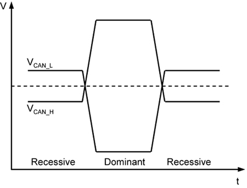
The CAN bus can have one of two logical states: recessive or dominant (Figure 2). In normal communication mode, the transceiver needs it’s maximum input current in the dominant state and its minimum in the recessive state. The currents needed for the I/O level adaption and for the remote wake-up capability can be neglected in this case, since they are provided by the microcontroller’s supply and the car’s battery, and are usually very small.
In the presence of a bus failure, however, the supply current can increase significantly, especially if the CAN_H bus line is shorted to ground. Most transceivers will limit the short-circuit current to a certain maximum value. In order not to risk a breakdown of the supply voltage, it is better to dimension the charge-pump output current for this case.
Taking the above into consideration, supplying a CAN transceiver with the proper power requires a charge pump that features an output voltage of 5V with the voltage tolerance specified in the devices data sheet, and a minimum output current capability to cover the CAN_H short-to-ground event.
Click image to enlarge
Figure 2: Voltage level of the CAN bus for recessive and dominant logic states
Example: Max13041 Transceiver supplied by the MAX1759 Charge Pump
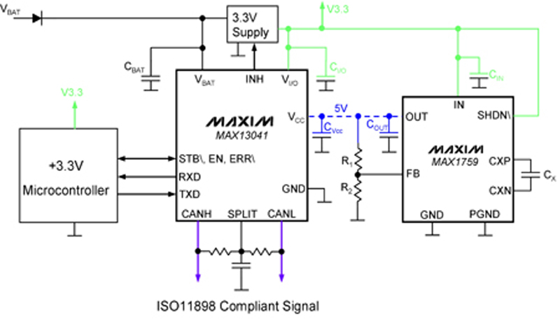
Although many conventional CAN transceiver and charge-pump devices are on the market, this article focuses on the MAX13041 HS CAN transceiver and MAX1759 buck/boost regulating charge pump to show how to solve the power-rail issue. The transceiver is supplied through the VCC pin. To provide ISO 11898 standard compliant CAN communication, VCC must be between 4.75V and 5.25V (normal operating-voltage range). This voltage is used to build the proper communication signal between the bus lines (CAN-H, CAN-L), and to supply the receiver stage when the IC is in normal mode.
The transceiver’s VI/O input enables the interface with 3.3V I/O microcontrollers so the correct voltage level can be established between the controller’s and transceiver’s receive/transmit stage (RxD/TxD). The VI/O pin can also be supplied by 5V, of course, when the application is communicating with such a controller.
The VBAT pin (usually connected to the car’s 12V battery) supplies power to a very-low-quiescent current wake-up detection circuit. This pin enables the MAX13041 to wake up from sleep mode on a CAN message. For a detailed description of all other pins, please refer to the MAX13041 data sheet.
In normal communication mode, the MAX13041 needs a maximum input current (VCC pin) of 80mA in the dominant state and 10mA in the recessive state (Figure 2, again). The currents into VI/O and VBAT can get neglected. In the presence of a bus failure, the VCC supply current can increase significantly, especially if the CAN_H bus line is shorted to ground. The Max13041 will limit the short-circuit current to IO(SC) = 95mA.
Taking the above into consideration, supplying the CAN transceiver with the proper power requires a charge pump that features an output voltage of 5V with the voltage tolerance mentioned above, and a minimum output current capability of 95mA.
Charge Pump Requirements
The MAX1759’s architecture allows the input voltage to be higher or lower than the regulated output voltage. However, in this application the charge pump operates as a step-up voltage converter only. When VIN is lower than VOUT, the charge pump operates as a regulated step-up voltage doubler. When lightly loaded, the charge pump switches only as necessary to supply the load, resulting in low quiescent current. Output voltage ripple does not increase with light loads.
For a detailed description of all features of the charge pump, please refer to the MAX1759 data sheet.
Implementing a 3.3V solution
The circuit in Figure 3 illustrates how easy it is to supply the MAX13041 with the charge pump. The MAX1759 is simply added to the VCC input of the CAN transceiver (see the blue dashed line), producing a 5V output voltage with the required tolerance and output current. This configuration allows the rest of the circuitry to be supplied by lower voltages. In this example, an external supply voltage of 3.3V (green) supplies the charge pump (IN), the microcontroller, and the VI/O level-translator voltage of the transceiver. The active-low SHDN input of the charge pump is pulled high, putting the part into it’s ON state. The detailed dimensioning of the input/output (CIN, COUT) and the flying capacitor (CX) is described in the MAX1759 data sheet.
Click image to enlarge
Figure 3: In this circuit, the MAX1759 charge pump supplies 5V to the MAX13041 HSCAN transceiver
Electromagnetic compatibility
Electromagnetic compatibility (EMC) can be a challenge to achieve with CAN applications, especially if they are supplied with a switching voltage regulator. The wiring harness of the CAN system is particularly problematic, as the CAN_H and CAN_L pins of the CAN transceiver are the interface to the bus network running into the entire vehicle. If care is not taken, one can encounter interference, or create interference, that propagates from the CAN supply, through the transceiver, over the bus wires into other ECUs, or into the neighboring cables of the harness. Such interference can cause miscommunication or malfunctioning of the transmitting or other control units in the system.
Because of this concern, we test the EMC behavior of the MAX13041 supplied by the MAX1759 charge pump and compare it to the behavior of the transceiver supplied by a filtered, 5V-supply. In this way we see both the impact of EMC interference from the charge pump and the pump’s robustness against interferences from the CAN lines propagating to the supply. In this test, we consider two domains: electromagnetic immunity (EMI) and electromagnetic emission (EME).
Immunity Testing (EMI)
The ISO 11452 specifications describe several methodologies for testing immunity to RF disturbances, including bulk current injection (BCI), transversal electromagnetic-cell (TEM-cell), stripline, and direct power injection (DPI).
We use the DPI method because of its high reproducibility (due to the use of a well-defined test board) and the relatively low test effort needed. The principle of the DPI test is straightforward: inject a certain AC voltage into the bus lines, modulated or not, and check the integrity of the transmitted data signal through the transceiver’s RXD pin. This method also facilitates comparison between different suppliers' designs and, moreover, is used by independent laboratories testing CAN transceivers (e.g., IBEE [Ingenieur Buereo fuer industrielle Elektronik]).
Test setup
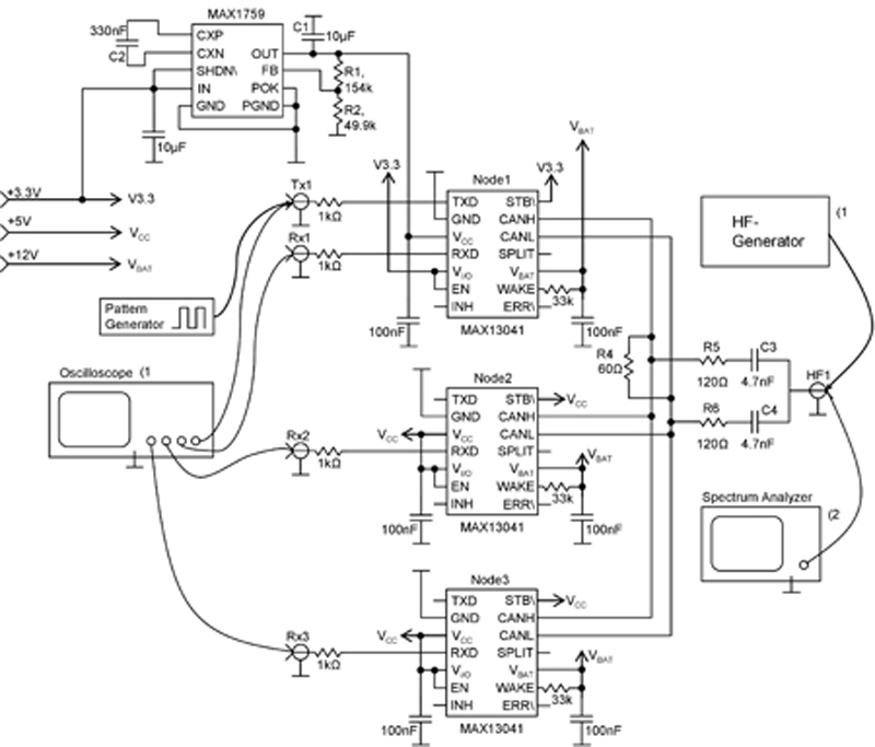
The test setup (Figure 4) consists of three identical transceivers soldered on a defined PCB, with one transceiver supplied by the MAX1759 charge pump. Node 1 operates as a transmitter for a bit pattern that simulates a CAN message to be received and monitored at the RxD output ports of all transceivers. For RF decoupling of outputs Rx1 to Rx3 and for the input TxD1, 1kΩ resistors are used. A buffer ceramic capacitor (C = 100nF) is used at the supply ports VCC and VBAT of every transceiver IC. The resistors at the wake-up pin have a value of 33kΩ. The devices are set to normal mode by tying the pins EN and the active-low STB high. The VCC voltage for node 1 is generated by the MAX1759 charge-pump circuit, which is supplied with 3.3V. The 3.3V supply was also used as the VI/O voltage of transceiver node 1.
The output capacitor C1 for the charge pump is 10µF; the flying capacitor C2 is 330nF; and the input IN pin is decoupled with a 10µF capacitor. In the test circuit, the bus termination is realized by a central termination using the 60Ω R4 resistor. Symmetrical RF coupling/decoupling is realized with the parallel RC combination of R5/R6 = 120Ω, C3/C4 = 4.7nF. The external 3.3V, 5V, and 12V supplies are provided by standard power supplies, filtered by a filtering network.
Click image to enlarge
Figure 4: Test setup for DPI and emissions testing
1) The oscilloscope is used for immunity testing only
2) The spectrum analyzer is used for emissions testing only
Test procedure
The test is performed with the MAX13041 CAN transceivers operating in normal mode. The first test run is done with all transceivers supplied by a standard VCC = 5V supply; at the second test run, one CAN transceiver is supplied by the charge pump (Figure 4). A pattern generator produces a square wave with a duty cycle of 50% to simulate a CAN signal (with permanent data alternation 0-1-0) of 500kbps on the TXD pin of node 1. An HF generator on the RF input (HF1) injects an amplitude-modulated (AM) AC voltage, with a certain frequency, corresponding to a power of 36dBm into the CAN lines to simulate the disturbances.
To evaluate immunity, an oscilloscope is used to compare the Rx signals of the three transceivers in the network while they are under the influence of the disturbances to the signal fed into TXD. A validation mask with a maximum allowed voltage deviation of ±0.9V and a maximum allowed time deviation of ±0.2µs is overlaid across the TXD signal-wave shape.
If the failure criteria is true (i.e., if one of the transceiver’s RXD signals is beyond the validation mask window), the injected RF power is reduced by 0.2dBm and the same test (at the particular frequency step) is repeated until the failure criteria is false. Then, the current power value is recorded and the next frequency step is adjusted. The test is carried out over a 10MHz to 100MHz frequency range.
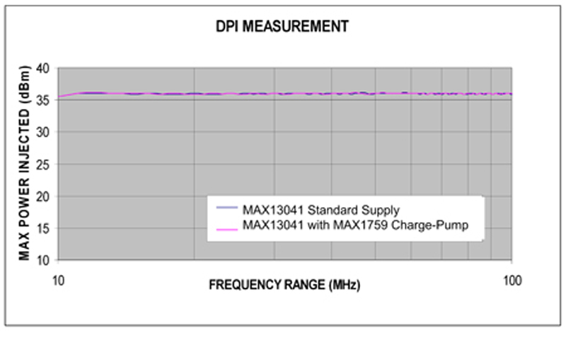
DPI test results
Figure 5 shows the test-result curves of the MAX13041 supplied by a standard 5V supply on VCC (blue) and the MAX13041 supplied by the charge pump (pink). The X axis indicates the frequency range, while the Y axis indicates the maximum power injected without failure.
The blue and the pink lines are almost identical. This indicates that the EMI behavior of the circuit is dominated by the CAN transceiver's EMI susceptibility and not the charge pump’s EMI susceptibility. Therefore, supplying the MAX13041 CAN transceiver with the MAX1759 charge pump does not significantly affect circuit performance when the circuit encounters any EMI.
Click image to enlarge
Figure 5: DPI test results
Emissions testing (EME)
The emissions test is performed on the same test board and test setup as the DPI test, except that the power injector (HF generator) is replaced by a spectrum analyzer. The test is again performed with the CAN transceivers operating in normal mode. The first test run is performed with all transceivers supplied by the standard VCC = 5V supply; the second one is performed with one CAN node supplied by the charge pump. The applied square wave on the CAN TXD input (simulating a transmitting bit stream of 500kbps) is maintained, and the emissions on the CAN lines are measured and recorded by the spectrum analyzer in the 100kHz to 1GHz frequency range. The oscilloscope is not required (Figure 4).
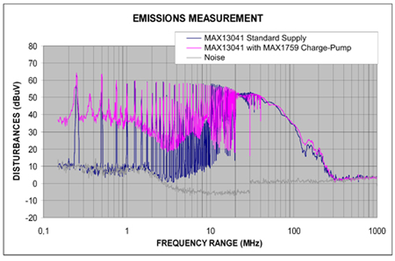
Emissions test results
Figure 6 shows the resulting EME curves of the MAX13041 supplied by the standard 5V supply on VCC (blue) and by the MAX1759 charge pump (pink). The X axis indicates the frequency range, while the Y axis indicates the level of the disturbances.
Here the peaks of the blue and the pink lines (one transceiver supplied by the charge pump) are almost identical to the lines for the MAX13041 with the standard 5V supply (blue). This shows that the emissions behavior of the circuit is dominated by the CAN transceiver's emissions compatibility, and not that of the charge pump. These test results indicate that it is possible to supply a CAN transceiver with a charge pump without significantly influencing the overall EMC behavior of the system. However, if transceivers or charge pumps of other semiconductor vendors are selected, it would be wise to run these tests on those specific products since each vendor’s product performance could be different.
Click image to enlarge
Figure 6: EME curves of the MAX13041 supplied by a standard 5V (blue) and by the MAX1759 charge pump (pink)
Conclusion
It can be challenging to achieve electromagnetic compatibility with CAN applications, especially if they are supplied by switching voltage regulators (charge pumps). However, this article demonstrates that the EMC behavior of the circuit is not significantly influenced by the charge pump. Thus, supplying a CAN transceiver with a charge pump for applications that require low-power, low-voltage operation at low cost is an option for system designers who do not have a readily available 5V power-supply rail.


