It has been more than 12 years since the first GaN-on-Si power transistors started in volume production
Figure 1: Pricing comparison between eGaN FETs and MOSFETs. Prices were for 1,000 pieces in February 2022
In many applications, such as lidar and space electronics, adoption of GaN has been extremely rapid. Lidar flourished as a result of the extremely high speed of GaN devices, which is more than 10 times faster than the aging silicon MOSFET. Space electronics has rapidly accepted GaN-on-Si power transistors due to its extreme radiation hardness, high performance, and small size compared with rad hard MOSFETs.
But what about other markets such as consumer products, computers, motor drives, and automotive. In each of those areas GaN devices have appeared in volume, although many designers are still on the sidelines. With more than 1,000 customers over just this past year, we have seen only 10% of first-time customers convert to repetitive customers within one year.
In this article, the most common reasons for some customers to be slower in their embracing what is clearly a displacement technology for their older silicon-based power MOSFETs will be discussed. Without going into the detailed statistics, a list of reasons, in order of frequency is derived. This list is based upon the understanding that some applications will place higher emphasis than others on certain characteristics of GaN. Our discussion is limited to devices rated at less than 400 V, as that is the application focus for Efficient Power Conversion (EPC) FET and IC products.
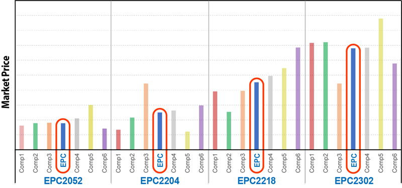
Misconception 1: GaN devices cost more than silicon devices
This is the most common misconception. In about 2015, the first GaN-on-Si transistors started appearing that were actually lower in price compared with power MOSFETs with the same on-resistance and voltage ratings. Since then, GaN transistor prices have continued to decline, while at the same time, the technology has improved and die-shrinks have been achieved.
In figure 1 is a comparison of prices for EPC’s 100 V eGaN FETs. This chart shows various on-resistance specifications for GaN devices and their MOSFET counterparts. Although medium volume pricing in February 2022 was used, it can be inferred that the same relationship should track to higher volumes.
At higher voltages, where the relative performance differences and size differential between eGaN FETs and MOSFETs is even greater than at lower voltages, the pricing of GaN devices is even comparatively lower.
Perhaps more interestingly, the comparable pricing ignores the fact that, at equivalent voltage and on-resistance, eGaN FETs are smaller and much faster than the comparable MOSFETs. The users get much greater performance at a comparable price.
Misconception 2: GaN devices are harder to use
There are two sub-categories to this misleading statement:
1. First, the statement refers to chip-scale packaging and its small spacing between terminals.
2. Second, the statement refers to the sensitivity of GaN devices to small parasitic inductances in a PCB layout.
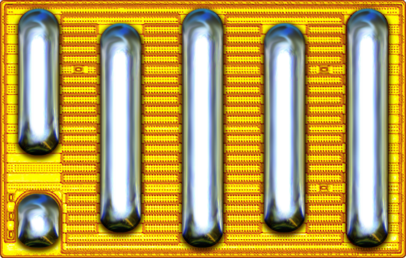
Chip-scale packaging, such as that shown in figure 2, can be challenging to use when the user’s prior experience is only with traditional power MOSFET encapsulated packaging, such as the PQFN.
Click image to enlarge
Figure 2: The EPC2204 is a 100 V, 6 mΩ(max) enhancement mode GaN-on-Si transistor in wafer level chip-scale format (WLCS)
WLCS formatted parts can drive finished PCB board costs higher due to requirements for tighter geometry. In addition, the exposed silicon substrate of the WLCS device upon which sits the active GaN transistor, is more susceptible to chipping during the manufacturing process.
However, there are offsetting advantages that translate into higher performance and lower cost end products. These advantages include smaller size, lower parasitic resistance and inductance, fewer reliability issues, and more efficient heat extraction when using top-side cooling. These reasons have led power system designers wanting to be leaders in performance to master high volume manufacturing using higher performing GaN WLCS products. Many electronic systems manufacturers (ESMs) have been audited and certified in these assembly processes as well. In fact, in some high performance or high-volume applications silicon ICs have adopted WLCS packaging.
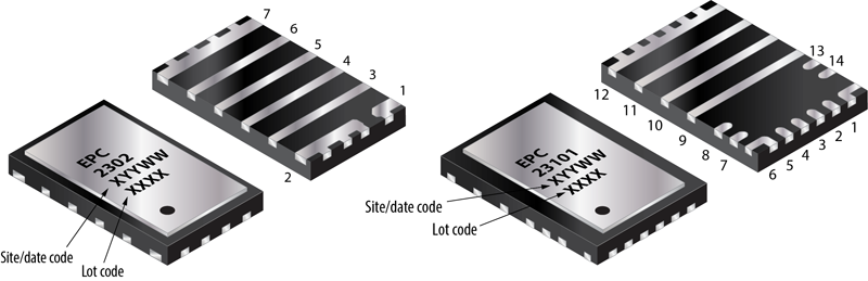
Recently, EPC introduced a family of packaged parts for those designs less inclined to adopt GaN due to manufacturing concerns about chip-scale packaging. On the left side in figure 3 is the EPC2302 eGaN FET. It is in a 3 x 5 mm PQFN package with 0.6 mm minimum spacing between terminals. The backside of the device is exposed for efficient heat extraction. On the right side of figure 3 is a companion integrated circuit, the EPC23101, which has all the necessary integrated circuitry to make a complete power stage circuit when combined with the EPC2302.
Another advantage for using the PQFN package is that several devices ratings (voltage, RDS(ON)) will be offered in a common footprint, allowing more flexibility in customer end-product designs.
Click image to enlarge
Figure 3: (left) The EPC2302 is a 100 V, 1.8 mΩ(max) enhancement mode GaN-on-Si transistor in a 3 x 5 mm PQFN package. (Right) The EPC23101 is a 100 V, 3.3 mΩ(max) high side FET including level shift, bootstrap, and low-side drive circuitry in a 3.5 x 5 mm PQFN
GaN devices are extremely fast. Their speed implies rapid changes in voltage and current that, when coupled with even a small amount of inductance, can cause unwanted overshoot and oscillations. These conditions can lead to overvoltage as well as EMI. There have been books and papers written that provide layout techniques that can reduce the parasitic inductances added in the PCB without adding cost to the design. Even better, products such as the EPC2152 [9] monolithic power stage integrate the various components that can be responsible for parasitic power loop, common source, or gate-loop inductances. Certainly, there will be more and more of these types of devices available that take the burden out of the design activity without compromise to performance or cost.
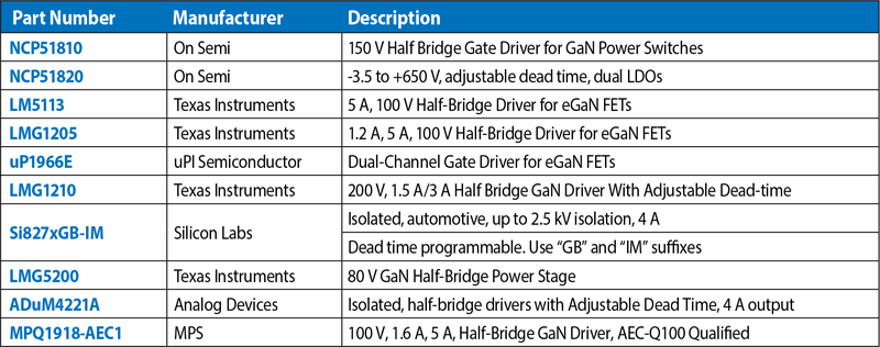
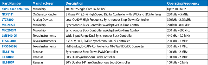
Misconception 3: GaN devices have limited numbers of compatible drivers and controllers
This misconception is being diminished every day. Table 1 lays out a list of GaN compatible half-bridge driver ICs. These ICs were specifically designed to work with GaN transistors and monolithic half-bridge products. Note that, if the designer uses monolithic power-stage ICs, such as the EPC2152 or EPC23101/EPC2302 chipset, no driver is needed.
Click image to enlarge
Table 1: GaN compatible half-bridge drivers as of February 1, 2022
Table 2 lists controller ICs that were designed for buck, and buck boost, circuits with GaN device’s fast switching capability in mind. There are other controllers available for motor driver and synchronous rectification applications. This table is constantly updated as new controller ICs are introduced to the market.
Click image to enlarge
Table 2: GaN compatible buck and buck-boost controllers as of February 1, 2022
Not having as long a history as MOSFETs, this list of GaN controllers is not as extensive as the list for aging MOSFET transistors, but the promise of higher performance and smaller size, with multiple products from which to choose, will tip the scale for new designs more and more in favor of GaN products.
In the future, separating the analog or digital controller from the driver will be the ultimate win-win with the taking advantage of the performance of monolithic GaN IC power stages and the richness of functions available in silicon.
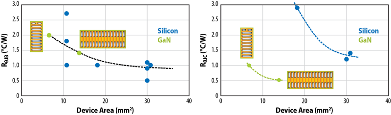
Misconception 4: GaN devices are so small that it is hard to extract the heat from the device
Shown in figure 4 is a comparison of the thermal resistances between GaN devices and silicon MOSFETs versus the area of the device. There is little difference between silicon and GaN devices in the ability to conduct heat through the PCB. However, as can be seen on the right side of figure 4, there is a significant difference in the ability to extract heat from the topside of the device. This difference is so significant that in cases where topside cooling can be deployed in a design, a GaN device will be five to ten times more thermally efficient, more than compensating for the five to ten times smaller footprint.
Click image to enlarge
Figure 4: Junction to board (left) and to case (right) thermal resistance comparison between GaN and silicon devices
Misconception 5: GaN devices have little or no proven reliability
GaN devices now have hundreds of billions of device hours in field applications with results that are superior to anything ever reported from MOSFETs. GaN transistors are in cars and in orbit around the Earth. Recent reliability studies have drilled into the fundamental physical mechanisms that wear out GaN devices. These studies have shown the benefits stemming from the stronger chemical bonds in GaN that lead to the wide bandgap and its superior reliability. For example, GaN devices are less sensitive to higher temperatures, and actually show improved lifetimes at elevated temperatures.
There is no example of an application that works for the aging MOFET that does not work even better using a GaN device.
Summary
Designers of power systems must contend with many constraints including performance, size, cost, and reliability. Recently, supply chain shortages have extended silicon component lead times out past 52 weeks, which adds another challenge for the designer. Designing with GaN devices can help reduce these component shortages.
GaN devices check all the boxes for a superior new product. They have superior performance, are easy to use, extremely small, highly reliable, and very affordable. Perhaps most important of all…they are also widely available with short lead times, thanks to a more efficient supply chain matched to this new-generation power device.


