Silicon Carbide Technology and Digital Gate Driving Pave Way for Electrification of Heavy Transport Vehicles
It has been estimated that the transportation sector offers greater potential for slashing greenhouse gas (GHG) emissions through electrification than buildings, industry, or any other sector
Among the most promising technologies in the mission to decarbonize emissions-intensive transportation vehicles are SiC-based power-management solutions supported by configurable digital gate driver technology.
The high power and voltage requirements of electric vehicles (EVs) of all types, including electric buses and other e-transportation power systems, require the higher efficiency of silicon carbide (SiC) technology to replace older silicon Field Effect Transistors (FETs) and Insulated-Gate Bipolar Transistors (IGBTs).
This combination delivers significantly better efficiency than silicon when electrifying some of the world’s biggest carbon dioxide (CO2)-equivalent GHG emission sources as measured in teragrams (Tg): buses (22.2), rail (37.6), and medium- and heavy-duty trucks (444). Key systems in these commercial transportation vehicles -- such as the auxiliary power unit (APU) in a train or bus -- can be reduced in size and operated with greater efficiency and reliability at lower cost using SiC MOSFETs that employ digital gate drivers to squeeze the most productivity from the least amount of energy.
Moving to 1700 Volt (V) SiC MOSFETs
The advent of high-voltage silicon carbide (SiC) MOSFETs has extended the technology’s benefits to support the power conversion needs of electrified commercial and heavy-duty vehicles, light rail traction and auxiliary power (see Figure 1).
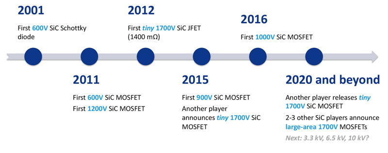
Click image to enlarge
Figure 1: Multiple vendors are now on the market with large-area SiC MOSFETs at the 1700 V class
Because these 1700V SiC devices have a tiny fraction of the switching losses found in competing silicon IGBTs, their switching frequency can be increased and the size of the power converter may be drastically reduced. The benefits are particularly valuable when operating under “light load conditions” (see Figure 2). An example is the use of a transportation APU to operate train doors that spend most of their time closed. SiC MOSFETs reduce conduction losses in this situation and, complementing the already low switching losses they deliver, remove the need for such thermal management measures as heat sinking.
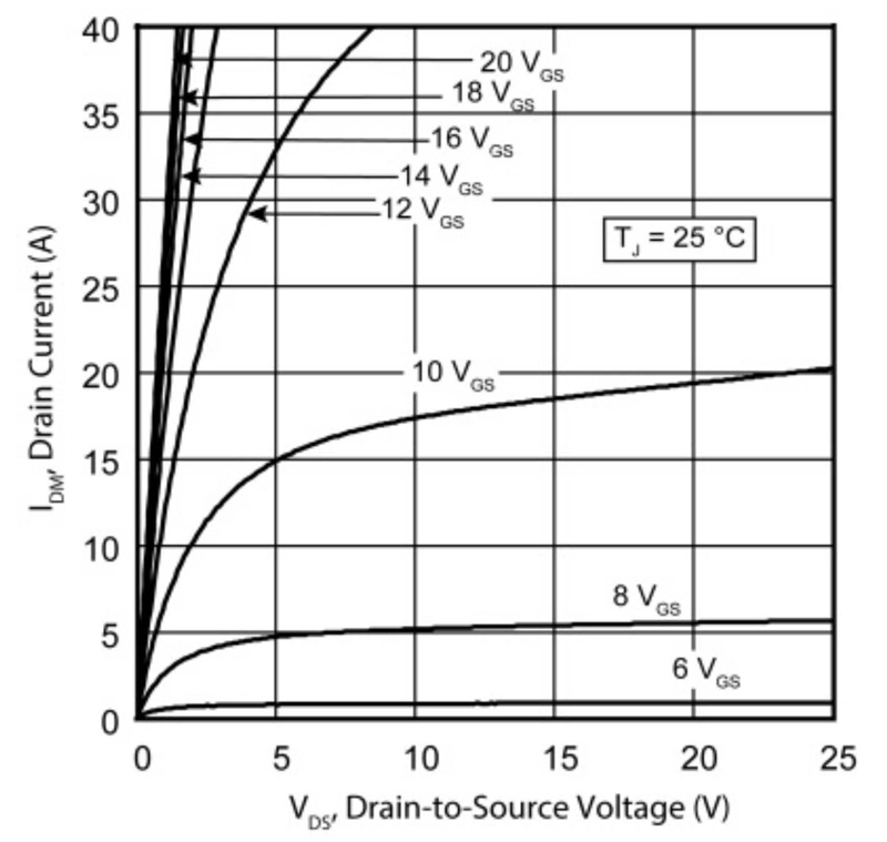
Click image to enlarge
Figure 2: The output curves show that unlike a silicon IGBT, the SiC MOSFET has no knee voltage, meaning the conduction losses are also lower at light load conditions. A vast majority of applications operate at light load most of their service lifetimes
Today’s higher-voltage SiC MOSFETs also improve reliability while reducing costs by simplifying circuit topology and reducing component count. The 1700V blocking voltage reduces the size of the power converter, and designers can also replace three-level circuit architectures with a much less complex two-level circuit that halves device count while streamlining control.
Designers should consider several critical factors when choosing SiC MOSFETs for a multi-megawatt application like heavy-duty transportation vehicles. One is the use of modular solutions based on a basic unit cell (also known as a power electronics building block or sub-modules).
Another consideration is the robustness of the SiC MOSFET’s intrinsic body diode. Designers should select devices that show no perceptible shift in tests of pre- to post-stress ON-state drain–source resistance (RDSon). This ensures they will not degrade after many hours of constant forward current stress when conducting reverse current and commutating the remaining energy following a switching cycle. SiC MOSFET test results should be carefully reviewed since some SiC MOSFET options show at least some level of degradation, while others go so far as to become unstable. The optimal SiC MOSFET choice will eliminate the die cost and power module real estate of an external antiparallel diode that would otherwise be required to solve the degradation problem. Even this solution, however, trades lower cost for potentially choppy body diode performance (some more choppy than others). This can be resolved by using digital gate drivers to adjust the SiC MOSFET’s turn-on parameters.
Digital gate drivers also are essential for mitigating the secondary effects produced by SiC MOSFETs’ faster switching speeds. These include noise and electromagnetic interference (EMI), limited short circuit withstand time, and overvoltage due to parasitic inductance and overheating.
Digital Gate Driving Unleashes Full SiC Capability
Standard analog gate drivers, even when modified, are inadequate for meeting the unique requirements of SiC technology. In addition to being designed from the ground up for these devices, digital gate drivers also enable designers to save months of development time by experimenting with configurations and re-using them for many different gate driver parameters such as gate switching profiles, system-critical monitors and controller interface settings. Being able to quickly tailor gate drivers to a variety of applications without any hardware changes cuts development time from evaluation through production. Control parameters can be modified at any point in the design process.
Digital gate drivers offer numerous valuable benefits. They can reduce drain-source voltage (VDS) overshoots by as much as 80 percent as compared to the traditional analog approach, cut switching losses by up to 50 percent and reduce time to market by up to 6 months. They make it possible to source/sink up to 20A of peak current and provide an isolated DC/DC converter with-low capacitance isolation barrier that can be used for pulse width modulation signals and fault feedback. In addition to robust fault monitoring and detection, these drivers also provide independent short-circuit response, and enable designers to control MOSFET turn-on and turn-off much more precisely than traditional analog gate drivers that only control turn-off slope through gate resistors for normal and short-circuit situations.
The augmented switching capabilities enabled by configurable digital gate drivers continue to evolve. The technology now provides up to two turn-on control steps compared to the single step of traditional analog drivers, and up to three turn-off control levels. Providing this “soft landing” during turn-off delivers the same benefits as tapping a foot on an antilock system’s brakes. Four levels of short-circuit settings deliver even more granular control over this secondary effect of SiC switching speeds, while addressing overshoot, ringing and turn-off energy, among other variables. These capabilities enable designers to meet the increasing demands of SiC applications, which require a combination of faster switching as well as more precise and dynamic, multi-step turn-on and turn-off.
Configurable augmented turn-on capabilities are especially valuable in applications such as motor control. When the rate of change of voltage (dV/dt) is too high it results in a shorter motor life expectancy and correspondingly higher warranty costs. Until higher-frequency motors are available, the only way to solve this problem with analog gate drivers is to reduce SiC speed, but this decreases efficiency. Only with digital gate drivers can dV/dt be fine-tuned to speedily achieve the most appropriate compromise.
Figure 3 summarizes the differences between analog gate drivers and the new digital generation.
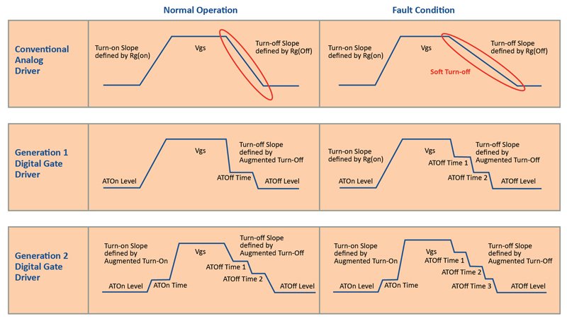
Click image to enlarge
Figure 3: Comparison of a traditional analog gate driver to two generations of digital gate driver technology
Creating a direct path from evaluation to production using digital gate drivers starts with a gate driver core and module adapter boards. Rounding out the ecosystem are a SP6LI low-inductance power module, mounting hardware and connectors to the thermistor and DC voltage, along with a programming kit for the configurable software.
The module adapter boards increase flexibility by enabling designers to quickly configure and re-use gate driver turn-on/turn-off voltages across many different suppliers’ SiC MOSFETs with different positive or negative voltage ranges, without any redesign. This is the case even if the SiC MOSFET was previously used with an analog gate driver. The designer simply reconfigures the digital gate driver and can immediately move the solution into production while continuing to mix and match gate driver cores and module adapter boards with the same accelerated path to production. Testing can begin immediately with an SP6LI low-inductance power module connected to a laptop computer and a phase leg. Keystrokes replace the laborious process of soldering gate resistors onto a board to change gate driver behavioral parameters.
Next Steps
The combination of 1700V SiC MOSFET power management solutions with digital gate driving technology will play a key role in the global mission to electrify heavy-duty transportation vehicles. It has extended SiC’s benefits to support these vehicles’ power conversion needs, while speeding and simplifying the path from design to production and creating new capabilities such as changing switching profiles in the field as SiC MOSFETs degrade. Packaged into total system solutions, this new generation of power management technology is making room for more paying passengers in electrified metro, subway, and other heavy transportation vehicles by enabling significantly smaller auxiliary power units while also dramatically improving the system design experience.