A look at the implementation of an 8-bit analog-to-digital converter (ADC) using a single IC
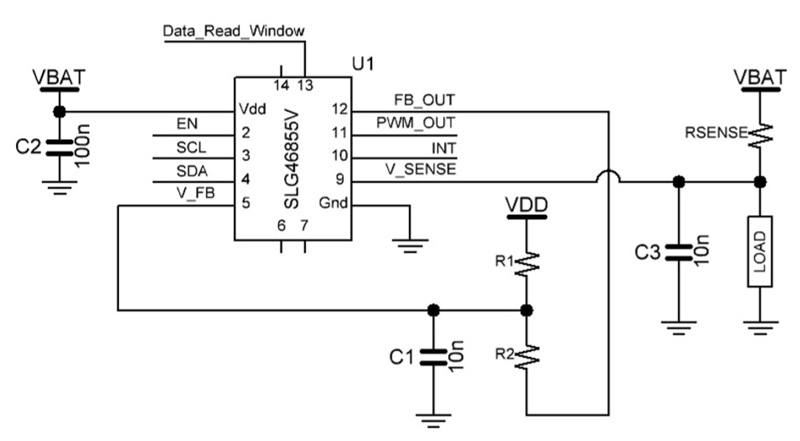
Figure 1: External circuit schematic
Dialog Semiconductor’s SLG46855V is able to sense load current and then interface with an MCU through an I2C connection. This ADC design provides current data to an MCU or SoC via I2C and can be customized to integrate other functions with available logic, all within a small 1.6 x 2.0 mm package. It can be used for various current sensing applications such as ammeters, fault detection systems, and fuel gauges.
The ADC is essentially comprised of an analog comparator and a Digital-to-Analog Converter (DAC). The comparator senses the input voltage vs the DAC output voltage and subsequently controls whether to increment or decrement the DAC input code, such that the DAC output converges to the input voltage. The resulting DAC input code becomes the ADC digital output code.
In this implementation, we create a DAC using pulse-width modulation (PWM) controlled resistor network. The PWM, when filtered, becomes our analog voltage. A distinct advantage of this approach is that it is easy to set the voltages which correspond to zero code and full scale (equivalently offset and gain) by simply adjusting resistor values of a resistor network. For example, a user can set it to ideally read zero code from a temperature sensor with no current (0 µA) corresponding to 4.3 V, and full-scale code at 1000 µA corresponding to 3.9 V.
A design consideration for this architecture is that an internal PWM frequency needs to be much faster than the ADC update rate to prevent underdamped behavior of its control loop. At the very least it should be longer than the ADC data counter clock divided by 256. In this design, the ADC update period is set to 1.3312 ms.
The flexible ADC is based on the design presented in the AN-1177.
An external resistor and capacitor network are used to convert a PWM into an analog voltage as shown in the circuit schematic in Figure 1. The values are calculated for the maximum resolution according to the maximum current the device will sense. To achieve this flexibility, we add resistors R1 and R2 in parallel to VDD and ground. A resistor divider divides down VBAT to the low side of the voltage range. The divider ratio for an expected minimum VBAT can be solved using the following equation.

The I2C commands require a start bit ([), control byte (0x10 (Write); 0x11 (Read)), word address (0xA5), read bit (R), and stop bit (]).
An example I2C command to read back the CNT0 counted value is written below:
[0x10 0xA5] [0x11 R]
The counted value that is read back will be the ADC code value.
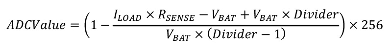
To test the accuracy of the ADC current sense design, the measured values at a given load current and VDD level were compared to a theoretical value. The theoretical ADC values were calculated with the following equation:
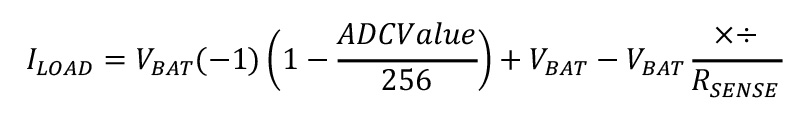
The ILOAD that correlates with an ADC value is found with the following equation:
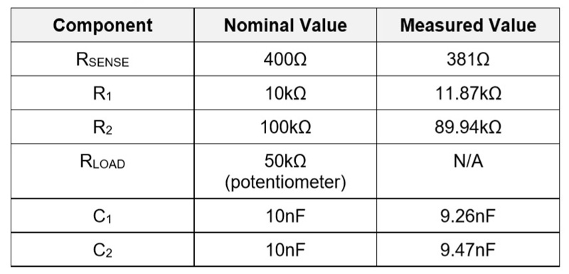
For the following results I used these component values shown in Table 1:
Click image to enlarge
Table 1: Component Values for Test Circuit
The resolution of the ADC value to ILOADconversion can be calculated by using equation 3 with the measured values in Table 1 and the ADC value set to 1. With a VBATof 3.9 V, the resolution is 4.96 µA/div.
To optimize the ADC current sense circuit to a minimum VDD level of 3.6 V with a maximum current of 1100 µA and a 381 Ω sense resistor, the ideal divider coefficient would be 0.884, based on the equation 1. With the values given in Table 1, the actual divider has a divider coefficient of 0.876. Since this is slightly less, it will allow for a slightly larger load current range so the ADC values are close to the full range but will not overflow. The actual divider value is calculated with the following equation:

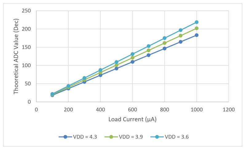
Below, there are the measurements taken of the circuit at three voltage levels: 4.3 V, 3.9 V, and 3.6 V. Theoretical values are rounded to the closest whole integer. There is a graph (Figure 2) displaying the correlation between the theoretical ADC values and load current at the different voltage levels.
Click image to enlarge
Figure 2: Graph of correlation between theoretical ADC values and load current
Click image to enlarge
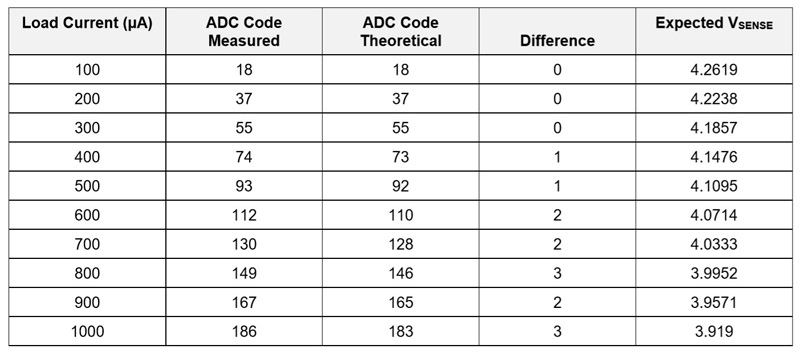
Table 2: Measured values with VDD = 4.3 V
Click image to enlarge
Table 3: Measured values with VDD = 3.9 V

Click image to enlarge
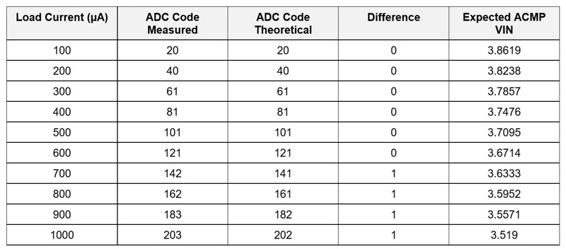
Table 4: Measured values with VDD = 3.6 V
The three voltage levels the device was tested models a full lithium-ion battery that discharges to its nominal level. Of the three voltage levels, it is observed that the device typically was more accurate at 3.9 V for the chosen external circuit. The difference between the measured and theoretical ADC values was only 1 decimal value off at load currents of 700 - 1000 µA. At the given voltage range, the measured ADC values were 3 decimal points above nominal conditions in the worst case. Further adjustments to the resistor divider can be made to optimize different VDD voltage levels.