SupIRBuck® online design tool makes it easy
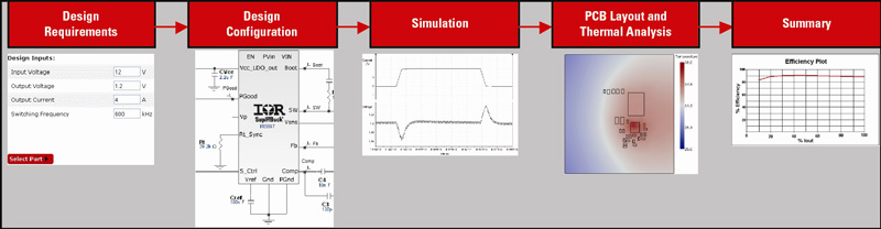
Figure 1: Five steps of working with the SupIRBuck® Online Design Tool
Fast and reliable design and evaluation of Point of Load (POL) circuits is a major factor to reduce the product development cost and time for electronics industry. Switching power supply circuits such as POLs form a big percentage of the electronic content of products and relatively high power nature of these circuits adds to the complexity of the evaluation and troubleshooting. Furthermore, in response to the expanding need for POL solutions many integrated circuits with variety of features are developed. Selection of the best fit among many options and optimal design of the application circuit is a major challenge for developers, especially digital specialists with limited experience of power circuits. SupIRBuck® online Design Tool is a comprehensive, accurate, interactive, and user-friendly tool for any developer to step by step effectively select the best fit among the SupIRBuck® family and design the application circuit. IR's SupIRBuck® regulators are highly efficient, easy-to-use, fully integrated synchronous buck converters. These regulators incorporate IR's high performance synchronous buck controllers and benchmark HEXFET® trench technology MOSFETs in a compact Power QFN package. This package is standard, easy to assemble, and scalable. The internal gate-drivers are designed to match the MOSFETs for the best performance and the feature-set for each part number are customized to provide the minimum external components. Thus, the solution is efficient, compact, rugged, and cost effective. Using this technology, the controller can operate over wide input and output voltage range and overcome the limitations of monolithic and discrete solutions to simultaneously improve efficiency and space. This approach provides enough flexibility for optimizing the converter for different applications with few external components. The current SupIRBuck® family includes more than forty seven members with 4x5mm and 5x6mm size packages, input voltage up to 27V and maximum continuous output current of 25A. The control engines are either voltage mode controlled PWM or constant on-time. SupIRBuck® design tool supports the most recent generation of SupIRBucks® also known as preferred parts. Design Steps with SupIRBuck® Online Tool The SupIRBuck® Design Tool is web-based and created on WebSIM® platform. User can create and track designs in an individual account and even share them. As the input, user enters design parameters, selects components, verifies the design by simulation, and specifies the PCB. On the output, user receives Bill of Materials (BOM), simulation results, bode plot, estimated efficiency and power loss, and thermal distribution on the board. Figure 1 shows the five steps of working with the tool. First, user selects desired features and enters the design inputs such as input voltage, output voltage, load current, and switching frequency. Then, the tool suggests a matrix of part numbers. The 1k budgetary price and efficiency at 10%, 50%, and 100% load for each part are listed, so user can select the price vs. performance among possible options. After the selection of part, the tool automatically designs the application circuit with the default design specifications (e.g., output voltage ripple and load transient response) and draws the schematic. The design includes selection of input and output capacitors, output inductor, and compensation values. User can override the default values and re-design the circuit.
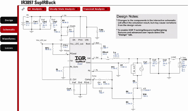
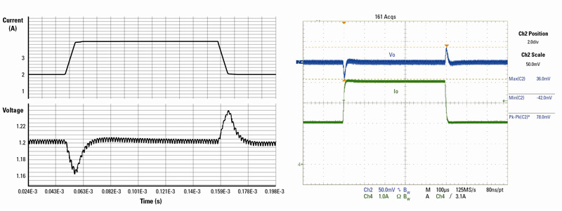
Once the schematic is designed, user can perform AC, steady state, and transient analysis. The performance of POL circuits, especially load transient response, cannot be described precisely with design equations. Thus, performing simulations are necessary for verification. SupIRBuck® online tool uses SIMPLIS® for electrical analysis. Although the model created for SupIRBuck® is a detailed switching model, the simulation can finish within few seconds. One great capability of this tool is defining the electrical specification and mechanical size of PCB and providing the option for the placement of components on the board accordingly. User can even add extra components on the board to create mechanical limitation as the actual PCB. After defining the PCB layout, user can perform analysis to obtain the power loss and the thermal distribution on the PCB. Finally, the tool generates a complete report of the design including schematic, BOM, electrical simulation results, efficiency versus load current, pie chart of power loss, and results from thermal analysis. In following, features of the tool are explained in more details with an example. Design Example An application with single 12V input voltage, 1.2V output voltage, 4A maximum continuous load current, and 600kHz switching frequency is selected as an example. The desired part should have dedicated pin for over-voltage protection, Enable input, PGood output, internal LDO, and input voltage feed-forward control. Thus, the tool suggests IR3897, IR3898, and IR3898. We choose IR3897 for the best price and higher efficiency up to 50% load. The design entries are set to target 120kHz target loop bandwidth and 30% peak to peak inductor current ripple. Figure 2 shows the designed IR3897 schematic. User can edit components and enter custom values or select a part number from the database. In the next step, electrical simulations are performed to evaluate the performance of the solution under common operating conditions. To demonstrate the accuracy of the tool, simulation results are compared against experimental ones from an IR3897 demo-board with identical schematic. For example, Figure 3 shows load transient response from the experimental and simulation. User can define the PCB and arrange the placement of components on the board after performing electrical analysis. In the "Board Definition" tab, one can define the size of the board, number of layers, and the thickness of the copper. For this example, the parts are arranged on the board to be identical to the IR3897 demo-board. At this stage, the thermal analysis can be performed. User has the option to specify the ambient temperature and air flow and its direction. For the given example, the thermal analysis is performed at 25°C and no air flow. Both experimental and simulation results show the maximum board temperature is about 37°C at Sync-FET of IR3897, where the maximum power is dissipating.
SupIRBuck® design tool estimates the total power loss of circuit and contribution of each component. The estimated total power loss for this example at 100% load is 633mW, which is very close to the measurement taken on the demo board at similar condition. The match of the simulation results with the experimental ones is another indication of the effectiveness of this tool in rapid and reliable selection, design, and evaluation of SupIBuck® circuits. www.irf.com


