Developing a low thermal resistance path for wide bandgap power transistors leadless packages
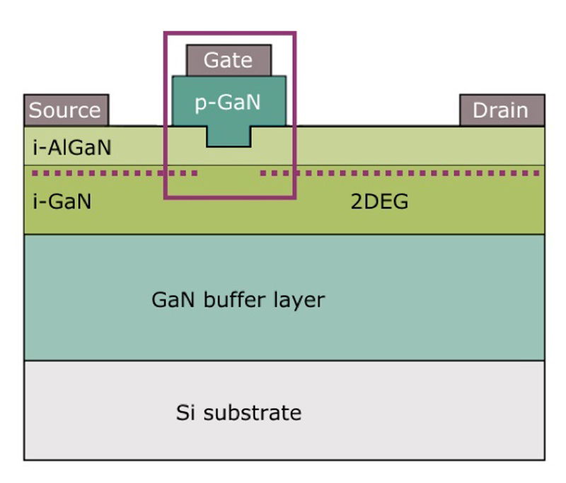
Figure 1: The GaN-on-Si wide bandgap HEMT structure
The demand for higher power density in many applications is driving the development of wide bandgap semiconductors. Compared to standard power transistors based on silicon, devices based on wide bandgap (WBG) materials such as silicon carbide (SiC) or gallium nitride (GaN) offer significant benefits. High electron mobility transistors (HEMTs), are being realized using gallium nitride on silicon (GaN-on-Si) platforms, to create power transistors that deliver higher levels of power density meeting future market demands.
The benefits of GaN
One of the main differences between a HEMT, like Infineon’s CoolGaN e-mode HEMT, and other types of transistors, is, that the HEMT is formed laterally instead of vertically. Together with the material properties of GaN such as a higher breakdown field (around ten times higher than in silicon), and an electron mobility that is almost twice as high as silicon, this results in a structure that delivers several advantageous features. A HEMT offers 10 times lower output charge and gate charge as well as zero reverse recovery charge, and a linear output capacitance characteristic.
These features enable new power conversion topologies, current modulation schemes, and deliver better efficiency in resonant circuits with fast and near-lossless switching. The indirect but much more impactful benefits for the end user include higher power density resulting in smaller and lighter power converter circuits with high efficiency, which leads to cost savings in operating expenses. Furthermore, the bill of materials (BOM) costcan be lowered, which results in a lower overall system cost. As shown in Figure 1, Infineon’s CoolGaN transistors are normally-off p-type enhancement mode HEMTs.
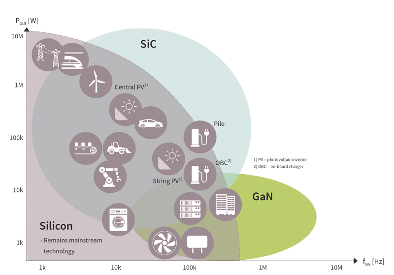
Especially in case of data centers where more power in the same (or less) space is favourable, there is a constant pressure to increase power density. The perfect solution to this design challenge is represented by Infineon's CoolGaN e-mode HEMTs, with reported figures showing that CoolGaN can return double-digit improvements in operating costs, while enabling a doubling in compute power per rack. In more general terms, Figure 2 indicates the application areas where gallium nitride, silicon carbide and silicon based power switches have a value proposition.
Click image to enlarge
Figure 2: Understanding where wide bandgap fits
In order to preserve the benefits of wide bandgap HEMTs, the devices need to be offered in surface-mount packages. The low parasitics of these packages ensure that the overall device performance is maximized. However, there may be concerns how the generated heat can be effectively dissipated from a surface-mount device mounted on a standard FR4 PCB. As you will read below, Infineon’s engineers have investigated and successfully modelled the optimum solution.
Thermal management
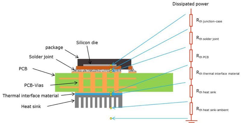
Despite the reduced losses of HEMTs compared to silicon power switches, the power they dissipate still needs to be removed and managed. No semiconductor device can operate at unlimited junction temperatures, and with every switching action the junction temperature will increase. If this process is not managed properly, the device will be destroyed, but removing heat from the junction incurs a number of physical barriers, most apparently because the junction is effectively buried deep inside the device. Figure 3 shows a model of the thermal path from the junction to an ambient atmosphere, for a surface-mount package. The thermal resistance of every step contributes to the overall thermal resistance (Rthja, measured in Kelvin per Watt, or K/W) from junction to ambient. To achieve the best performance, low thermal resistance is desirable.
Click image to enlarge
Figure 3: Thermal model of a leadless package soldered to a PCB
Distributing copper around a multilayer PCB typically involves the use of plated through-holes, or vias, connected with copper tracks. A matrix of vias beneath an SMT package can provide an effective thermal path to a heatsink. Intuition may indicate the type of via pattern to use, but to avoid any presumptions, Infineon engineers have conducted extensive research into this and presented the results in an application note [B. Schmölzer, F. Schnoy; “Thermal performance of surface mount semiconductor packages, Infineon Application Note, March 2018].
The results below were gathered by developing a range of PCB designs and using a test jig to accurately measure the Rthja. The same solder area was used in all cases, only the amount of copper below the solder mask and in the inner PCB layers was varied. A general trend emerged, showing variations between designs.
The referenced application note also covers two packages used for GaN, namely DSO and TO-leadless (TOLL) which are described as follows.
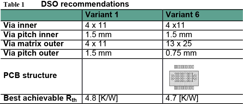
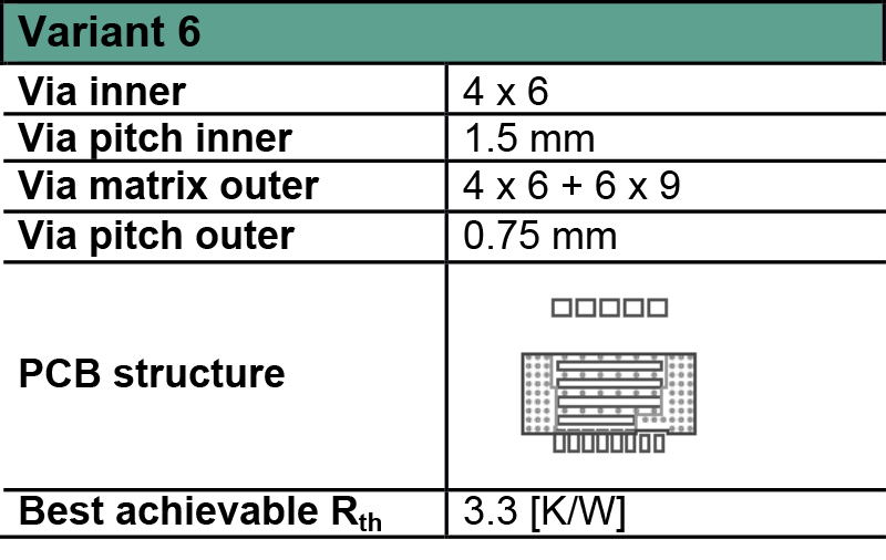
DSO package
8 different via patterns were investigated. Variant 6 is recommended, unless the design has space constraints, in such a case variant 1 is recommended.
Click image to enlarge
TO-leadless (TOLL) package
Table 2 shows the preferable via pattern for the TOLL package used for GaN considering cost and performance.Different to the DSO package TOLL shows a clear and strong dependency on the density of the vias.
Click image to enlarge
Conclusion
When using wide bandgap HEMT devices in an SMT package, it is important to consider the thermal management of the device(s), in order to maintain performance and maximize efficiency. As outlined in the article, the use of via patterns in FR4 can significantly help to reduce the overall resistance of the thermal path from junction to ambient.
Infineon Technologies