BYLink is a simple and effective way to deliver scalable safety and power solutions that enable customer platform integration
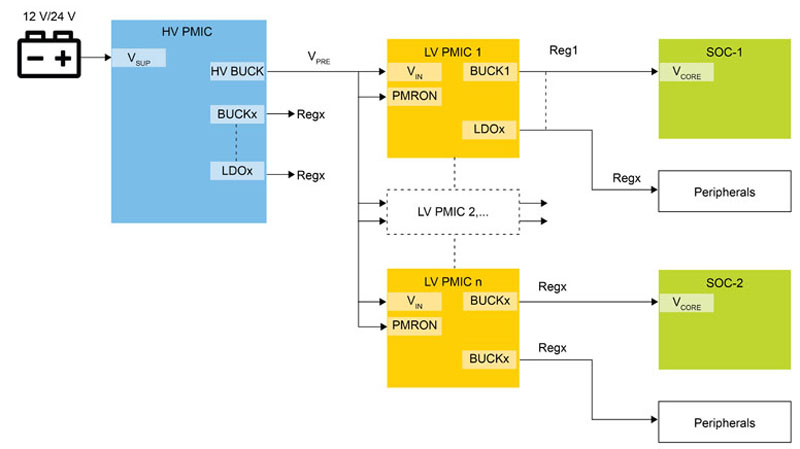
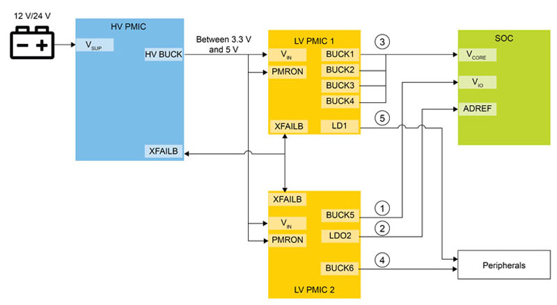
Figure 1: General concept of high and low-voltage PMICs connected together
In automotive systems, the 12 V and 24 V supply from the battery is used and derived in multiple supply rails to satisfy the system power demand. NXP’s portfolio of safety PMICs with embedded system features can be classified in two main categories: the high-voltage PMICs (HV PMIC) and low-voltage PMICs (LV PMIC). The HV PMICs are the PMICs directly connected to the 12 V or 24 V battery. The LV PMICs are the PMICs supplied with 5.5 V maximum.
The BYLink concept sees HV PMICs and LV PMICs connected together to deliver the required number of supply rails for the system with the capability of expanding the number of rails by adding low-voltage PMICs. The HV PMICs and LV PMICs share the same IPs making the two different PMIC families consistent and easily understandable. Furthermore, similar state machine and register architectures are used to increase consistency and software reuse from device to device within the families. Figure 1 illustrates the general concept.
In Figure 1, the HV PMIC connected to the battery delivers 3.3 V or 5 V from the pre-regulator and supplies the LV PMICs. As shown, the number of LV PMICs can be extended to deliver multiple supply rails to the SoCs and peripherals. Also, in the HV PMIC, several regulators (Buck and LDOs) can be used for the system. The limitation of the number of PMICs connected to the HV Buck will come from the current capability of the VPRE which is up to 15 A in the BYLink portfolio. Another advantage of this type of architecture is the spread of the power dissipation across the different LV PMICs. Concentrating a high number of rails in a single device can create hot spots on the board and approach or exceed the thermal shutdown of the device.
The complexity of the system is also linked to the number of SoCs and peripherals to supply. Most of the SoCs in the market require a specific, and well-defined order in sequencing the power up and power down of the rails. The power-up and power-down sequence is easily configured in the PMICs with the OTP block. As soon as the LV PMIC is powered, the OTP block will send an order to start the ramp up/down of the various regulators available in the LV PMIC. The duration between each regulator can also be configured to fine-tune the sequences in time. One LV PMIC may not deliver the complete supply rails to one SoC because of power dissipation constraints and in order to optimize the power trees.
Additional regulators in another LV PMIC may need to be connected to the same SoC, as shown in Figure 2. LV PMIC1 has 4 phases configured in multiphase to deliver higher power to the SoC core. The SoC has a specific requirement to start first with VIO, then ADREF, and finally VCORE. In this context, BUCK5 needs to start first, followed by LDO2 and finally Buck 1, 2, 3, 4 at the same time (simplified as BUCK1). Finally, the peripherals will be powered using BUCK5 and LDO1. To respect the timing and be sure the sequence will be synchronized between the two LV PMICs and the HV PMIC, the XFAIL B pins are connected. This connection allows the sequencer of the three devices to start at the same time, and the OTP will play the sequence according to the configuration stored on each device. The flexibility offered by the OTP block allows the customer to start different regulators after several µs or ms if it is required. The sequence is completely automatic and will be executed each time the devices are powered by the VPRE.
Click image to enlarge
Figure 2: LV PMICs connected to same SOC
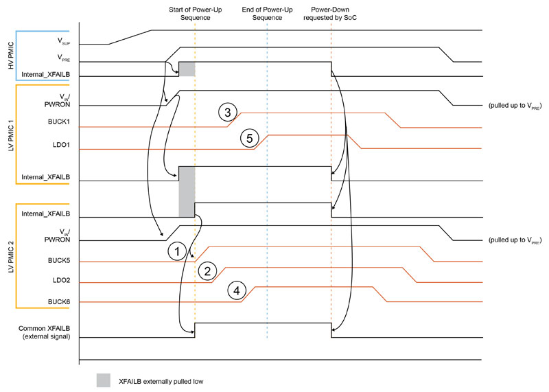
Figure 3 shows the timing diagram of the power-up and power-down sequences. The power-down sequence is configured to be the reverse of the power-up sequence but can also be changed by software if this is required. It simplifies the design of the power tree compared to discrete solutions where customers need to connect the PGOOD output of each regulator to the Enable input of the next regulator, or the use of an external and additional sequencer to manage the timing aspects.
Regardless of how many devices are needed to supply an application’s microcontroller and peripherals, a BYLink system can power-up and power-down seamlessly as one device because of device synchronization.
Click image to enlarge
Figure 3: Timing diagram power-up/power-down sequences
Safety, scalability and extended safety concept
Power management is one aspect of the system constraints, but functional safety is also an area that can be difficult to handle in such complex systems. Hardware engineers must satisfy the technical safety requirements for the system. Some of these requirements are directly reported to the PMICs, including:
• Voltage monitoring of the safety-related supply rails
• Monitoring of the SoC with an external Watchdog
• Hardware error monitoring of the SoC
• A safe-state control mechanism, redundant with the microcontroller, to transition the system to safe state in case of failure
In BYLink PMICs, these safety mechanisms are implemented, and each device exists in different safety flavors (QM/ASIL B for LV PMICs, or QM/ASIL B/ASIL D for HV PMICs). This facilitates the safety scalability at platform level thanks also to the pin-to-pin and software compatibility between devices. With the same physical device ( pin to pin compatible), the safety scalability is managed by activating or deactivating safety mechanisms with OTP ( one-time programming memory). The direct consequence is an increase or reduction of the global diagnostic coverage.
Differences are mainly around the latent failure metric (LFM) where we add the analog built-in self-text (ABIST) from QM to ASIL B, and logical built-in self-test (LBIST) from ASIL B to ASIL D. Other safety mechanisms, such as the watchdog’s complexity, are changed. Challenger Q&A watchdog is provided for ASIL D PMIC, while a simpler watchdog is enough for ASIL B devices. The BYLink concept solves some key aspects of the safety architecture and, by consequence, highly facilitates the integration.
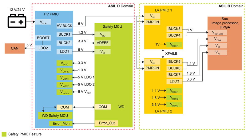
Figure 4 shows a complete BYLink solution, including safety MCU, SoC and peripherals. In this BYLink system, each of the PMICs has its own voltage monitoring. The HV PMIC is designed and configured to meet the highest safety level metrics for ASIL D while the LV PMIC1 and 2 can meet ASIL B at the maximum. The safety MCU is monitored by the HV PMIC (WD and Error_Out) with ASIL D capability. HV PMIC is in charge of transitioning the system into safe state thanks to its
safety output in case of critical failure. In our example, the deactivation of the CAN communication.
Click image to enlarge
Figure 4: Complete BYLink system solution
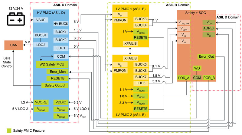
Starting from this architecture and moving towards a solution with only one SoC that has the safety and the computing capability of the two microcontrollers/SoCs shown in Figure 4, customers can still keep the same BYLink safety concept.
Figure 5 keeps the same power management configuration for clarity, but it could be different if additional power is required. Here, the BYLink concept with the HV PMIC ensures an ASIL D island with the safety processor in addition to the complete synchronization of the power-up and power- down sequences. The ASIL B domain is still managed by the LV PMICs. Expanding this solution to a concept where a full and complete ASIL D system is required, the “only” change that must be operated at system level in term of safety is the monitoring of the LV PMICs supply rails. To achieve that the regulators outputs from the second stage LV PMIC are now monitored by the front ASILD PMIC. The HV PMIC keeps the watchdog and error out monitoring with ASIL D capability. Latent failures check is performed by ABIST and LBIST and the capability to transition the system into a safe state if critical failures are detected is still provided to the HV PMICs.
Click image to enlarge
Figure 5: BYLink concept with 1 SoC (safety + computing)