Designing for efficiency and reliability from renewable
Solar electricity generation is becoming a viable alternative energy source, due to burgeoning energy costs. Up until 2007, the German solar market was the world’s largest solar market driven by a law encouraging the use of renewable energy through incentives (the “Energieeinspeisungsgesetz”).
Generating electricity from sunshine is taking the next step in market adoption, as the financial crisis seems to have been overcome. Panel prices have dropped further, and especially PV inverters have become a bottleneck for new installations. Earlier this year, the supply of PV inverters was so short that, for example, SMA in Kassel, the largest supplier of PV inverters with >38% market share worldwide, published an open letter to their customers on their website, apologizing for the shortage. As the markets in general seem to ease a bit, the same is not true for PV systems – other markets are taking the lead in terms of growth rates, in particular the USA and the emerging countries, as well as our European neighbours.
Click image to enlarge
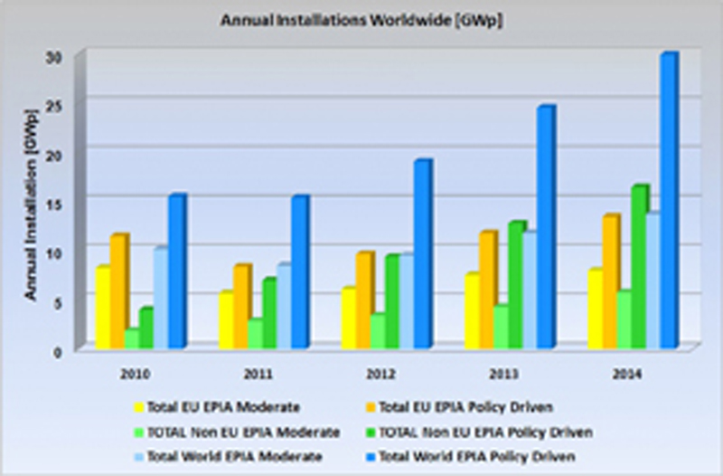
Expected market development
(Source: European Photovoltaic Industry Association, Update 2010)
It is interesting to note that there is still a large gap between the “Policy Driven” market development, which would be in line with the targets for renewable energy shares of the various countries, and the “moderate” scenario, which is based on assumptions of manufacturing capacities and historic market development.
Some other countries have taken the lead from Germany: in 2008 Spain had the largest amount of newly installed solar plant. Large growth in installed solar capacity is expected to come from Italy, France and the USA. The demand driven by these incentives has stimulated an increase in production capacity. The start of the recent world economic crisis and the sudden withdrawal of incentives from the Spanish solar market in 2008 have led to the supply of solar silicon exceeding demand at historic prices resulting in a price reduction of around 40%-50%. This brings photovoltaic technology closer to so-called “grid parity” where the cost of solar electricity equals the prevailing market price for electricity paid for by the consumer. Grid parity is now expected to occur sometime before 2015 for Germany.
Solar modules generate a DC voltage. A solar inverter converts this DC power into AC power which is then connected to the electricity grid. This article explores the new trends in solar inverter design. One important trend is to use higher power levels. Solar power farms with a peak capacity of over 100kW are becoming more popular. This trend is also seen for lower powered systems: the average power here is increasing from 5kWp to 10kWp.

Click image to enlarge
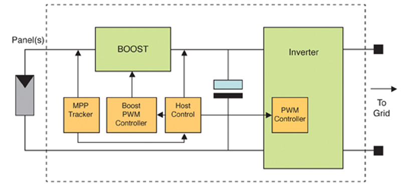
Figure 1: A popular solar inverter topology: boost + H-bridge
For solar inverters, one very popular topology is the boost plus H-bridge topology, which is a two-stage, non-isolated topology. The first stage is a boost stage which increases the variable output voltage of the modules (e.g. in the range 100V – 500V) to a higher intermediate voltage, which must be more than the actual peak mains voltage (e.g. 230V x √2 OR >325V). This boost stage has second important function. To maximize efficiency, solar modules need to be operated to generate the maximum possible power. The power curve of a solar module is given by multiplying the output current and the output voltage characteristics. There is a maximum point in the power characteristics known as the “maximum power point” or MPP. This precise point varies with factors such as the type of module, temperature of the module and the shading of the module.

Click image to enlarge
Figure 2: (Left) I-V characteristic of PV panel; (Right) P-V characteristic of PV panel
The input stage of the inverter tracks this maximum using a software technique called “maximum power point tracking” or MPPT, with the help of customized algorithms.
The second stage of the inverter converts the constant intermediate voltage into a 50Hz AC voltage which is fed into the mains supply. The output is synchronized with the mains supply phase and frequency. Since this stage is connected to the mains supply, it must achieve certain safety standards, even under fault conditions. In addition to this, there is a new draft proposal of the VDE 0126-1-1 linked to the Low Voltage Directive which requires that solar inverters should actively support the mains supply network in case of reduction in power quality which minimizes the risk of a more general power blackout.
Click image to enlarge
Block diagram of a PV inverter with the panels connected at the left side, and the grid on the right side
Under current regulations, it is permissible to design an inverter that protects itself by simply switching off in the case of a power outage. However, if solar inverters become popular and provide a significant share of the generated power, simply switching off the connected solar inverters when there is a power outage could cause a larger mains blackout, as one inverter after the other switches off and rapidly reduces the power available to the network. So the effect of the new draft directive will be to improve the stability and power quality of the mains distribution network at the cost of a slightly more complex inverter output stage.
Solar inverters need to be reliable, to minimize the cost of maintenance and downtime. These inverters need to be efficient, to maximize the amount of electricity generated and a considerable amount of effort is made by the designers of solar inverters to maximize the efficiency.
There are many ways to improve the efficiency of a boost converter. The boost converter can be operated in continuous or boundary conduction mode (CCM or BCM), leading to different optimization approaches. In CCM mode, one major source of losses is caused by the reverse recovery current of the boost diode. Here, silicon carbide diodes or Fairchild STEALTH™ diodes are generally used. BCM mode is more often used in solar inverters even if CCM mode is generally recommended for such power levels. The reason for this is that the forward voltage of the diodes used in BCM mode is a lot lower. BCM mode has a much higher ripple current in the EMI filter and the boost inductor. Good high frequency design of the inductor is one solution.
Looking closer at the current through the boost inductor, in continuous conduction mode the current never goes to zero but ripples around a relatively high input current, with the ripple being a smaller percentage of that input current. However, this means that the current in the diode will see an abrupt decrease when the main switch turns off, hence the need for a very fast rectifier with minimal recovery charge. When the converter is operated in boundary conduction mode, the current reaches zero in every switching cycle, and switching off the rectifier happens much softer. In combination with a silicon rectifier with very low recovery charge, like Fairchild’s STEALTH™ diodes, highest efficiency is reached. Still, the current ripple is much larger now, and that can be improved with an interleaved converter, where two phases are operated out of phase, and their ripple currents will partly cancel. The resulting current ripple at the output is significantly lower. In conclusion, the combination of an interleaved boundary condition mode boost converter like Fairchild’s FAN9612 and STEALTH™ diodes, highest performance can be achieved, as well as a very cost-effective solution.
A new approach is to interleave two boost stages instead of using one boost stage. This halves the currents flowing through each inductor and each switch. Further, the interleaving removes the input ripple current over a wide operating input range as the ripple current from one stage cancels out that of the other. Controllers such as the FAN9612 interleaved BCM PFC controller can handle solar boost stages without any problem.
There are two choices for boost switches in the inverter: IGBTs or MOSFETs. For input stages requiring switch voltage ratings of higher than 600V, fast switching 1200V IGBTs such as the FGL40N120AND are commonly used. For input stages where voltage ratings of 600V/650V are sufficient, MOSFETs are used.
Designers of the output H-bridge stage have historically used 600V/650V MOSFETs. New draft regulations have led to a renewed interest in using IGBTs in this area. These new regulations require four quadrant operation of the output stage.
In grid-connected applications like PV inverters, the grid quality is becoming more and more a concern, since these devices move power into the grid, by advancing the phase and / or the voltage, and that can lead to local overvoltages or increases in frequency. New regulations require the PV inverters to “control” the grid voltage, in an effort to keep both the voltage (230V +/-10%) as well as the frequency within tight limits (49Hz...51Hz), hence the need for the output stage of the PV inverter to be capable of operating in four quadrants, both delivering as well as absorbing energy. This requires the IGBTs in the inverter stage to be more robust and switching faster.
MOSFETs have built-in body diodes that have poor switching performance compared to the co-packaged diodes used in IGBTs. New field-stop IGBTs can switch voltages at a rate of 10V/ns which greatly improves the turn-on losses compared with older versions. The excellent soft recovery performance of the integrated diodes helps to reduce EMI caused by the high di/dt levels exceeding 500A/µs. For 16kHz-25kHz switching, IGBTs such as the FGH60N60UFD are recommended.

Click image to enlarge
Caption:Figure 3: Solar Inverter Trend: interleaved BCM Boost + three level Inverter
Another trend in the design of solar inverters is to increase the input voltage range, which results in a reduction in the input current at the same power level, or an increase in the power level with the same level of input current. Higher input voltages result in the need to use higher rated IGBTs in the range of 1200V, resulting in higher losses. One way of getting around this problem is to use a three-level inverter.
This trend is driven by efforts to increase the system efficiency, by connecting more panels in series, but also by new panel types, e.g. thin-film cells, that typically show a higher ratio of no-load voltage to voltage at the MPP. In inverter design, the target is to have maximum efficiency at the point where the string connected at the input has maximum power output, but the input structure must also be capable of surviving a higher input voltage in case of no power transfer to the grid, a no-load condition.
The high input voltage is divided into two by using two electrolytic capacitors in series. The midpoint is connected to the neutral line. 600V switches can now again be used. The three-level inverter can switch between the three levels: +Vbus, 0V and –Vbus. In addition to being more efficient than a solution built from 1200V switches, the three-level inverter has the additional advantage that the output inductors are much smaller.
For unity power factor, the function of the three-level inverter can be explained as follows: During the positive half-wave Q6 is always on, Q5 and Q4 are always off. Q3 and D3 form a buck converter which generated the output sine wave voltage. If only unity power factor is needed, Q5 and Q6 can be implemented as 50Hz switches using a very slow, very low Vce(sat) IGBT such as the FGH30N60LSD. If the power factor needs to be lower, Q5 and Q6 must operate at the switching frequency for a short time. The Diodes of Q3 and Q4 should be fast and soft recovery diodes. Q3 and Q4 could either be implemented as a fast recovery MOSFET such as the FGL100N50F or as fast IGBTs (FGH60N60SFD).
Based on these observations, it is likely that the three-level inverter topology will become popular for non-isolated inverters with power levels above 5kWp because of the possibility of achieving efficiencies of over 98%.


