In modern power conversion applications, utilizing switching power devices deadtime has been a necessary evil with which designers have learned to live to ensure reliable and worry-free operation
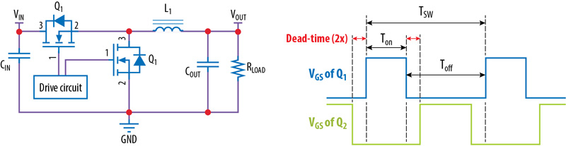
Figure 1: Deadtime in a synchronous buck converter
Deadtime is the delay needed between the turn OFF and turn ON of two devices when an overlap in ON times would result in cross conduction currents. A typical example for a synchronous buck converter where the simultaneous conduction of Q1 and Q2 would result in a short on the input voltage (VIN), which can lead to additional losses, higher operating temperatures and even failure in extreme cases is shown in Figure 1. This overlap is not caused by the controller itself, since even with zero overlap in the controller signals, mismatches between drivers, and FETs could result in an effective negative deadtime.
To avoid this overlap situation, a control deadtime is inserted by the controller on the gate signals to the gate driver. The intent of this control is to ensure that the effective deadtime is always positive. The control deadtime is determined by some initial calculations, sufficient guard-banding, and thorough testing. With this preset deadtime, the application will work in most situations with a significant amount of effective deadtime, so that in the worst-case condition the overlap will still have positive effective deadtime.
The main effects that need to be considered in analyzing deadtime are:
- Propagation delay mismatch on the gate drivers
- Differences in supply voltage between high side and low side
- Differences in the gate resistor values
- Mismatch of turn-ON and turn-OFF times on the FETs
- Diode reverse recovery time and variation in recovery time
It is clear from this list that calculating the perfect control deadtime is not an easy task as all these parameters can change because of manufacturing tolerances and operating temperature, as well as voltage and current levels of each device.
One of the main contributors to deadtime variation is the body diode reverse recovery time, and since this effect is absent in GaN devices, the difference between control and effective deadtime required by GaN devices is much smaller than for silicon MOSFETs.
Impact of deadtime on losses
Deadtime losses are often discussed in the context of GaN FETs, as the losses in the third quadrant of operation during effective deadtime are higher than the body diode losses of a Si MOSFETs. However, to have a full picture, all the contributors to losses during this event need to be considered, which include:
- Third quadrant conduction losses
- Output capacitance losses
- Reverse recovery losses (for Si MOSFET only)
- Reduced voltage hard switching turn ON (partial ZVS)
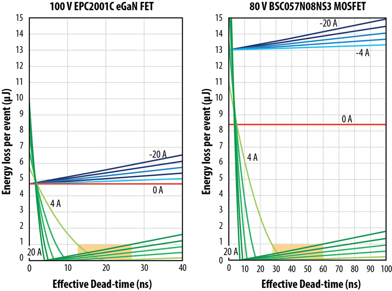
A detailed description of these effects is provided in, and an overall view of the effects on losses of deadtime for a half-bridge block are given in Figure 2 (in this analysis turn-ON and turn-OFF losses are not included, as they are not dependent on deadtime).
Click image to enlarge
Figure 2: Calculated deadtime losses per cycle versus deadtime for both eGaN® FET and MOSFET in a 60 V application (-20 A to +20 A in 4 A steps). Note the difference in horizontal scale between the two graphs
When considering the deadtime between the high-side turn OFF and the low-side turn ON, depending on the sign of the current, there are different loss contributors to consider:
- For negative current (current entering the half bridge) at turn OFF, third quadrant conduction on the high side starts and losses increase linearly with deadtime. At the end of the deadtime, the low side turns ON and during this hard switching event both COSS and reverse recovery (for the MOSFET) losses occur. These losses are shown in blue in Figure 2 and, in this case, to minimize losses deadtime should be kept as small as possible
- For positive current (current entering the half bridge) the effects are load-current dependent. If there is enough energy in the inductor to commutate the voltage completely, lossless zero voltage switching (ZVS) turn ON can be achieved. If not, the device will start to experience partial ZVS. Once this switching event is complete, third quadrant conduction can start, and losses increase linearly with deadtime from there. These losses are shown in green in Figure 2 and, in this case, there is an optimum deadtime, which is load-current dependent
The opposite situation occurs during the complementary deadtime between low-side turn OFF and high-side turn ON.
When comparing MOSFET to GaN devices it can be observed that
- Self-commutating energy to achieve ZVS is about half for GaN FETs due to lower COSS
- EOSS and ERR losses are about a third in GaN vs. MOSFET
- Third quadrant losses increase about 2.5 times faster in GaN vs. MOSFET due to higher diode-mode voltage drop, although these losses are a minor contributor when compared to the other three losses (partial ZVS, EOSS and ERR)
In conclusion, even with higher third quadrant conduction losses, a more detailed analysis shows that GaN FETs will not only be able to operate with a smaller deadtime, but will have overall lower deadtime losses.
Impact on control
The previous analysis highlighted that with GaN FETs losses can be reduced and utilize a smaller deadtime. Using short deadtimes has advantages on its own that can be seen at the application level.
In hard-switched converters, deadtime can improve control characteristics for high frequency and high step ratio converters.
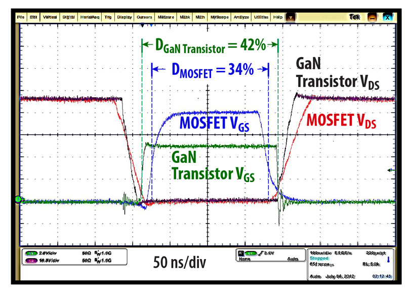
In resonant converters, the device output charge is proportional to the energy needed to achieve full ZVS. A reduction in energy can then result in reduced deadtime, providing a larger delivery period and lower RMS currents as shown in Figure 3.
Click image to enlarge
Figure 3: Effective duty cycle comparison between GaN FET and Si MOSFET resonant converter operating at 1.2MHz
Impact on motion
In motor drives, reducing deadtime will reduce the distortion created during zero current crossing eliminating undesired distortion and higher order harmonics as shown in Figure 4. This not only reduces audible noise, but also reduces the RMS current, thus greatly improving system efficiency. The deadtime is in fact responsible for the 5th and the 7th harmonics on the current waveform. These harmonics convolute in of the 6th harmonic of the torque applied by the motor to the load, and the 6th harmonic on the torque is responsible for undesired vibration and heat generation in the motor winding. When comparing current waveforms in Figure 4, the lower total harmonic distortion of the case with low deadtime increases the effective motor torque constant Kt [Nm/A], which in turn is responsible of a more efficient system operation.
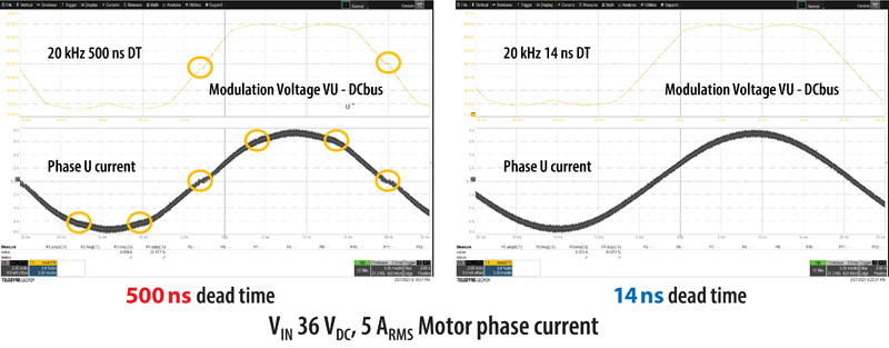
Click image to enlarge
Figure 4: Comparison of deadtime effect on zero-crossing distortions in a sinusoidal motor drive
Moreover, in motor drives applications, if the deadtime reduction is coupled with PWM frequency increase, the overall system efficiency effect can be increased as shown in Figure 5, where the same motor is operated at same speed and load but with different PWM frequency and deadtime. The effect of the deadtime reduction is visible in the Torque and in the nmotor rows. Torque is higher with lower deadtime, and motor efficiency is higher.
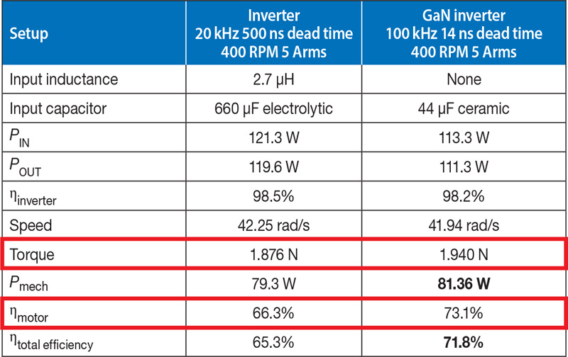
Click image to enlarge
Figure 5: Combined effect of deadtime reduction and PWM frequency increase on a sinusoidal motor drive
Conclusion
Deadtime is an important consideration in power electronics designs, and the improved Figure of Merit of GaN FETs versus Si MOSFETs allows operation with much smaller deadtimes. Minimizing this unwanted phase of operation allows designers to minimize losses at the component level and to optimize system level efficiency and operation. Although not quite able to eliminate it, GaN FETs deliver a strong blow to ever-present deadtime.