Two-switch forward converter: operation, FOM, and guidelines for device selection
This technology also competes with Zero Voltage Switching (ZVS) LLC topologies
The two-switch forward converter is quite popular with ATX power supplies/silver boxes in 150 W to 750 W output power levels, and also competes with Zero Voltage Switching (ZVS) LLC topologies. It is a hard-switched topology and does not operate in ZVS mode. But for that very reason it offers the benefit of having no body diode conduction. The input voltage seen by the MOSFETs used in this power range is the output voltage of a Power Factor Correction (PFC) converter, as required for any supply with output power ≥ 65 W. This voltage is typically 380 V to 400 V. During turn-off the MOSFETs may see an additional spike coming from leakage inductance energy, though it is clamped by the fast recovery diodes.
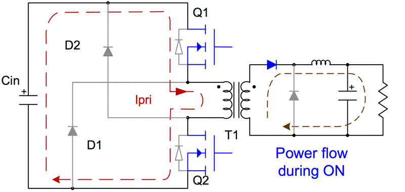
The basic operation is as follows: Figure 1a shows transistors Q1 and Q2, which turn on together transferring energy through the transformer primary into the secondary. On the secondary, the forward rectifying diode conducts, transferring the energy into the output filter and load.
Click image to enlarge
Figure 1a: Power transfer stage of operation
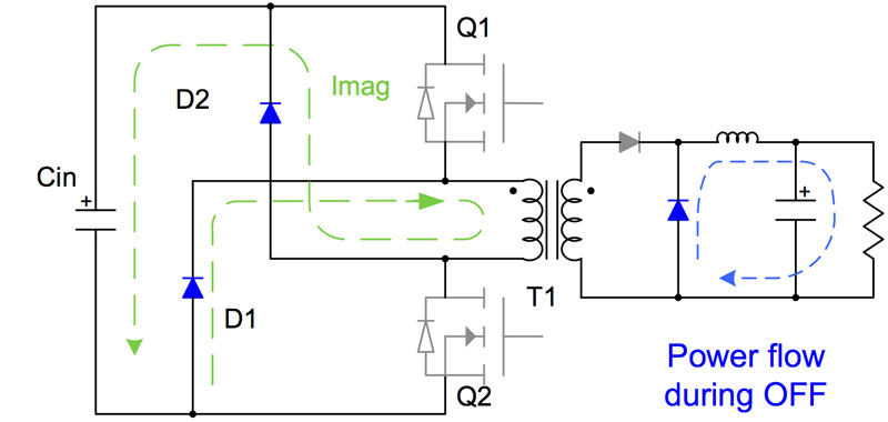
When transistors Q1 and Q2 are turned off, the transformer magnetizing current flows through the now forward biased diodes D1 and D2 and back into the source as shown in Figure 1b. The diodes conduct until all magnetizing energy in the primary, along with energy stored in the leakage inductances, is returned to input supply. Since diodes D1 and D2 clamp the input voltage, no snubber circuit is required. Any overshoot beyond the input voltage needs to be managed with proper circuit layout to minimize stray inductances. On the secondary, the freewheeling diode conducts as shown, transferring the output inductor energy to the load.
Click image to enlarge
Figure 1b: Power flow from output cap to power load
During the non-power delivery cycle of the primary, proper transformer reset time is achieved when the ON time is less than its OFF time (duty cycle is less than 50 percent). In other words, the primary winding itself acts as the reset winding. Having the OFF time longer than the ON time will always reset the transformer.
Dual Switch Versus PFC Converter, FOM, and Power Loss
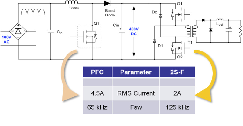
Figure 2 compares power losses of the two-switch forward converter to the single-switch PFC front-end converter in a 400 W power stage. The MOSFETs in the two-switch forward converter carry half the current, and switch at twice the frequency (125 kHz versus 65 kHz, typical). With this doubling of the frequency, the switching losses become a more dominant factor in the overall Figure of Merit (FOM) and power loss measurement.
Click image to enlarge
Figure 2: PFC converter versus a two-switch forward converter
To illustrate further, consider a TO-220 / TO-220F device with a maximum power loss of 8 W. Assume that this is an optimum choice for a PFC application. By optimum it is implied that conduction losses are approximately 40 % to 50 % of the total losses at rated power. Would it also serve as an optimum solution for the two-switch converter that follows? The answer is a definite no. In the two-switch topology the Coss / Qoss and Qsw would contribute approximately 87% of the total losses and the remaining would be conduction losses. Such unbalance between conduction and switching losses is highly undesirable for efficiency and cost. The reason why conduction losses are less than what would be seen in a single-switch PFC converter, is that each MOSFET used will have half the current of a single-switch PFC circuit, while switching at twice the frequency.
In any switching circuit there are two kinds of switching losses. The first is due to the Vds x Ids crossover that happens during turn-on and turn-off. These losses are weighted to what we call “Qsw,” which is the combination of the Qgd and the Qgs and represents the effective switching charge of the MOSFET. The crossover-related switching losses are a function of both load and switching frequency.
The second switching loss is associated with the charging and discharging of the MOSFET output capacitance Coss. In ATX power supplies, the popular two-switch forward converter follows the PFC converter having an input voltage ~ 400 V. As a result, the output switching loss can be a significant portion of the total losses. The Coss / Qoss of the device is a very important loss, especially at light loads where switching losses trump conduction losses. This loss is essentially independent of load and Qoss, along with Qsw, needs to be taken into account when selecting the appropriate MOSFET. An application-specific FOM based on loss contributions will look like:
Conduction losses (Rds(on)) + Switching losses (Qswitch) + Output losses (Qoss)
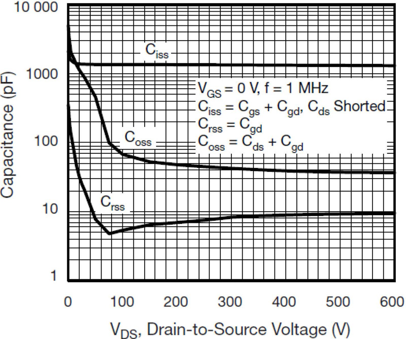
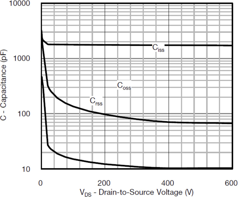
The Coss of a high-voltage MOSFET varies considerably with the applied VDS. This variation is much wider for high-voltage superjunction power MOSFETs (Figure 3a) than for planar types (Figure 3b). To account for the non-linearity of the output capacitor, Poss = ½ Co(er) x V2 x Fsw may be used as an approximate loss equation. The energy-related capacitance Co(er) is the effective capacitance that has the same stored energy and same losses as the integrated Coss of the MOSFET (0 V to VDS) and is provided in the datasheets. It may be pointed out that output capacitor related losses, which constitute a significant part of the total loss equation in any high voltage topology, are not taken into account in the industry standard FOM RDS(on) (typ) * Qg (typ). However, they are integral to the application specific FOM used in this analysis for device selection.
Click image to enlarge
Figure 3a: Super Junction technology capacitive plot
Click image to enlarge
Figure 3b: Planar technology capacitive plot
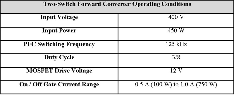
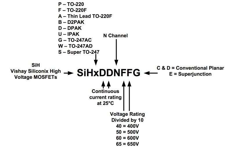
With this in mind, we have developed a list of components that we feel will achieve the highest efficiency for a two-switch forward converter based on typical operating conditions to ensure the most efficient design possible. Each MOSFET has a target loss of less than 0.5 % of the total converter loss. So, for a 400 W ATX power supply, the losses would be no more than 2 W per device. Table 1 illustrates the operating conditions assumed for such a power supply. The list of recommended devices includes an “x” in the “Package” location. For the same set of electrical characteristics, a number of package options may be available per device. The packages used will depend on the power level as well as what MOSFET real estate is allowed. Figure 4 defines the packages, current rating, voltage, and device technology of the different part numbers. With many package options available, Table 2 lists the recommended maximum power rating for the different package offerings.
Click image to enlarge
Table 1: Two-switch forward converter design conditions
Click image to enlarge
Figure 4: Part numbers definition

Click image to enlarge
Table 2: Maximum power levels based on package type


