Analysis of SMPS and Rectification: Inductor Violations
The inductor is a vital component of switch-mode power supplies, but choosing the wrong value could cause problems
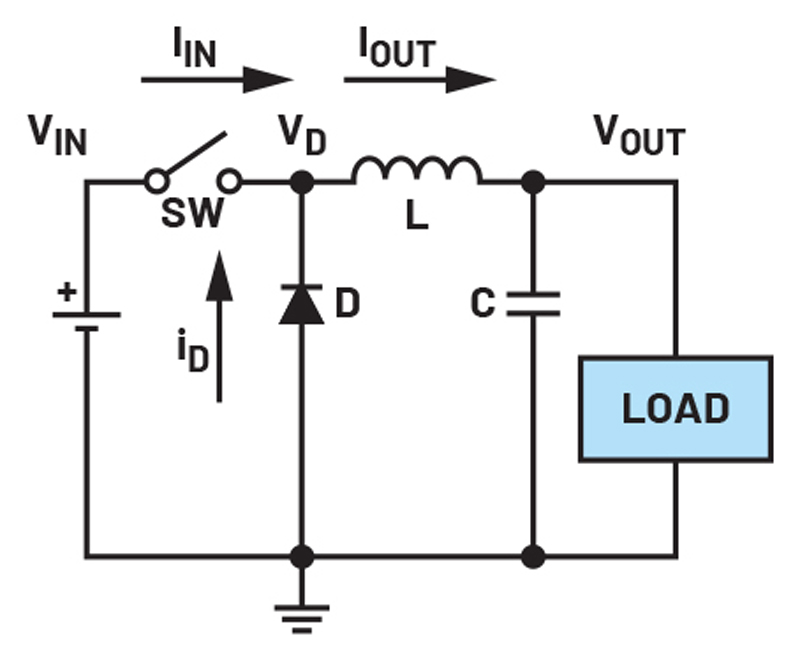
Figure 1. Simplified buck converter power stage
Every SMPS works by storing energy in an inductor and utilizing pulse width modulation (PWM) techniques to obtain the desired output. The guiding principle of these converters is the volt second balance law, which dictates that when operating in a steady state, over one period the average current of an inductor must be zero. This means that the inductor must discharge all the current its to red in the charging stage before another period begins.
This article uses buck converters to demonstrate common design errors. Four components make up the power stage of a buck converter: the inductor, the output capacitor, the top FET as represented by a switch, and the bottom FET, which is represented by a diode (see Figure 1).
The voltage across the inductor is given by: VL= L diL/dt. This voltage is the difference of the switch node from the output voltage. When the top FET is on, VListhe difference between the input voltage and the output voltage. When the top FET is off, the difference is 0 V minus the output because the switch node is grounded. diL/dt (or ∆iL) is the change in inductor current over time, commonly referred to as the inductor current ripple. When the top FET is closed (and the bottom FET is open), the inductor stores energy in the form of magnetic flux as the current through the inductor increases. When the top FET is open and the magnetic field collapses, a path to ground is formed by the bottom FET, allowing current to still flow to the load as it decreases. The output capacitor is used to smooth out the output ripple and help maintain the desired output voltage. The output voltage of a buck converter is given by VOUT = DVIN, where D is the duty cycle and is defined as the percentage of the time out of the total period where the top FET is on and charging the inductor.
When designing an SMPS, the right inductor value must be chosen to ensure an acceptable inductor current ripple (∆iL). It is recommended that the inductor ripple should be between 30% and 40% of the applied load current for buck converters. This range is considered to be optimal as it is big enough to capture and deliver an accurate signal to the current-mode control feedback system, but not too big that the power supply goes into discontinuous conduction mode (DCM). DCM is a state where the current ripple is too large, forcing the current to go below 0 A to maintain the load current at the desired value. However, once hitting 0 A, the diode inside the FETS no longer conducts, keeping the current from decreasing below 0 A. A general way to select the correct inductor can be obtained by the formula:
This formula shows that switching frequency and inductance are inversely proportional, meaning with higher frequencies, the charge time is reduced, allowing proper operation with a smaller inductor (saving footprint size and cost).
Saturating the Inductor
One of the most common and catastrophic errors in SMPS design is neglecting the current saturation rating when selecting the power inductor. When the current through the inductor exceeds the saturation current rating, the core of the inductor saturates, meaning that the magnetic field generated will no longer increase proportionately to the current drawn. This disrupts the volt second balance law, leading to a loss of linear characteristics in both the inductor current ripple and the output voltage ripple. When the iron core saturates, it loses inductance rapidly, behaving more as a resistor than an inductor. Since the effective series resistance (ESR) of the inductor increases, and the practical inductance decreases, the change in current is forced to increase to satisfy volts second balance. The peaking observed in the saturated current waveform is due to the exponential increase in the current slope. This current peaking carries over to the output voltage, leading to more noise and voltage spikes. The noise and voltage spikes can potentially damage downstream components if the voltage spikes too much and exceeds a downstream component’s maximum voltage rating, as well as degrade EMI performance.
Furthermore, with high current fluctuations, the inductor experiences rapid hysteresis loss leading to excess heat dissipation of the inductor, as well as audible noise. This excess heat can damage other nearby components, especially the regulator chip.
Inductors should be chosen with a current rating at least two times greater than the expected maximum current. When calculating the maximum current, it is important to account for the inductor current ripple as well as the load current drawn from the output. The inductor data sheet will show at what current the inductance drops by 10% to 30% of its original value, which is where saturation is defined. Choosing an inductor with the proper saturation current rating will result in normal operation of the system, as seen by a linear current through the inductor in Figure 2. The output voltage spikes will disappear, as seen in Figure 3. Finally, the system will operate at a much lower temperature, stressing the device less and improving the lifetime of the device.
Click image to enlarge
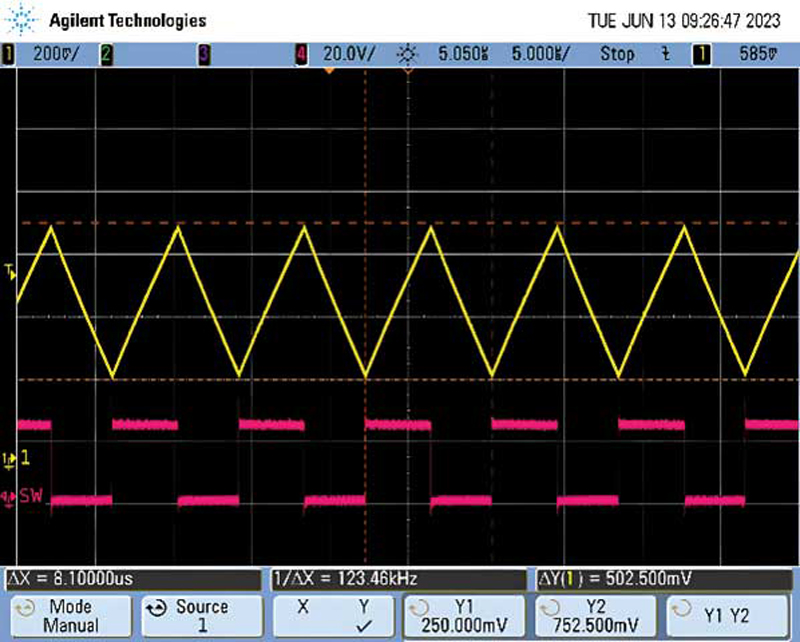
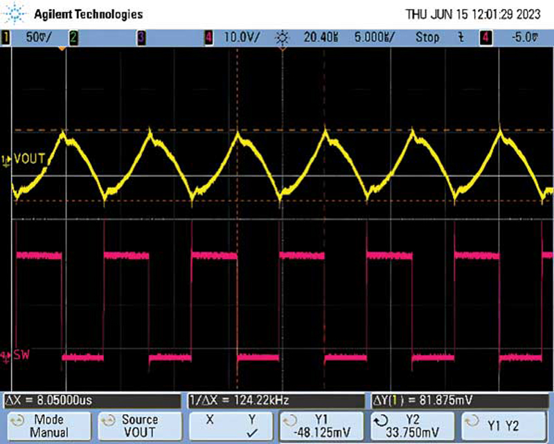
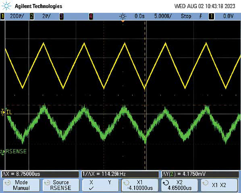
Figure 2. Nominal inductor current waveform
Click image to enlarge
Figure 3. Nominal inductor output ripple
To fix this issue, an inductor should be chosen that will provide a current ripple of about 30% to 40%. Doing so will reduce the magnitude of the inductor current ripple and bring the device back into CCM from DCM, as seen in Figure 6. This will improve the output voltage ripple as well and remove the voltage spikes.
Complications of an Undersized Inductor
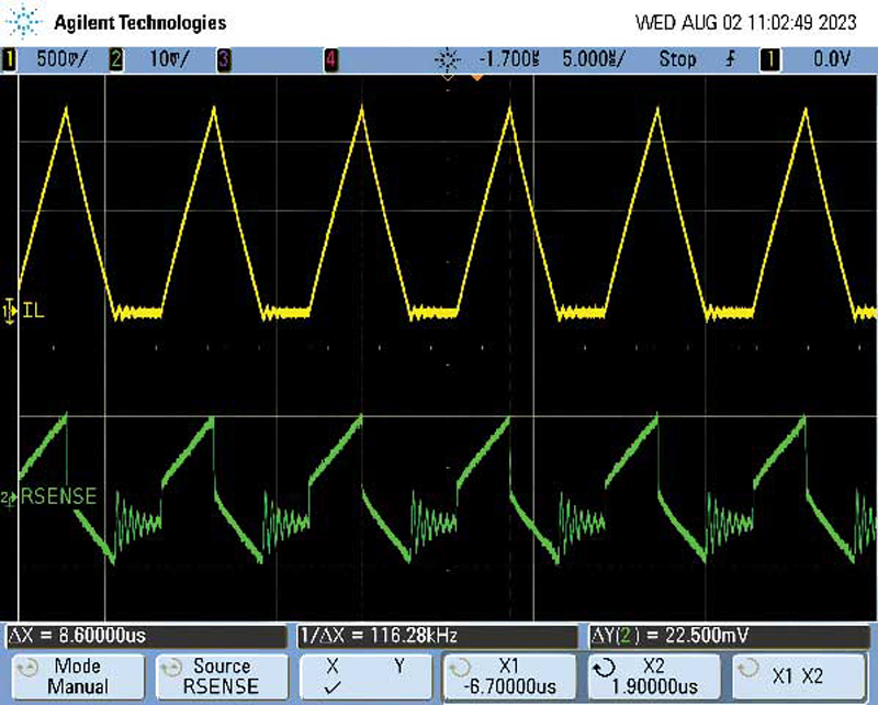
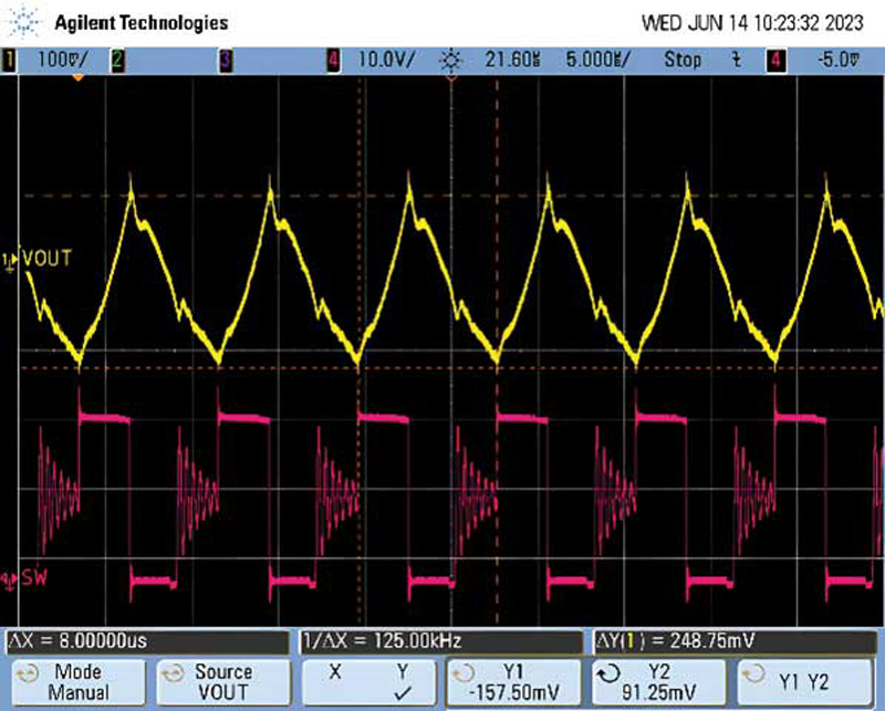
Smaller inductors save footprint space. However, if the inductor is too small, the ripple current will be large and will force the converter to go into DCM, which is undesirable for SMPS because the device will be less efficient and display worse EMI performance. This degraded EMI performance can be seen in the presence of ringing in the switch node, caused by parasitics as well as the LC tank (creating a resonant circuit), which can be seen in Figure 4. This ringing will carry over into the output voltage, leading to a larger ripple and more voltage spikes, as seen in Figure 5. Furthermore, the power supply is no longer in continuous conduction mode (CCM), and the derived SMPS output formulas no longer apply.
Click image to enlarge
Figure 4. Undersized inductor output waveform. Ringing can also be observed in the switch node if the inductor current is inaccessible
Click image to enlarge
Figure 5. Undersized inductor current waveform. The ringing present in the current and RSENSE indicate the power supply is in DCM
Click image to enlarge
Figure 6. Nominal inductor current waveform
Complications of an Oversized Inductor
The downstream electronics connected to an SMPS typically have specified supply voltages with an associated tolerance. If the ripple on the voltage rail is too large, it will drastically affect the operation of the system. One way that designers often try to mitigate this ripple is by increasing the size of their inductor. However, if the inductor is sized too big, the current ripple along with the output voltage ripple decreases significantly. Although this sounds desirable, it will lead to issues with the feedback system, and can also result in a much slower transient response. A small ripple will make it extremely hard for the series sense resistor to detect changes, distorting the usual triangular waveform that is passed into the feedback loop. When the inductor current ripple is small, the signal-to-noise ratio (SNR) deteriorates. This results in the feedback loop registering noise as the signal from the inductor, resulting in unwanted instability at the output, which manifests itself as jitter as seen in Figure 7.
Click image to enlarge
Figure 7. Jitter caused by the instability in the output. The waveform shown with the persist feature is the oversized inductor output waveform. The highlighted waveform is captured with the nominal inductor
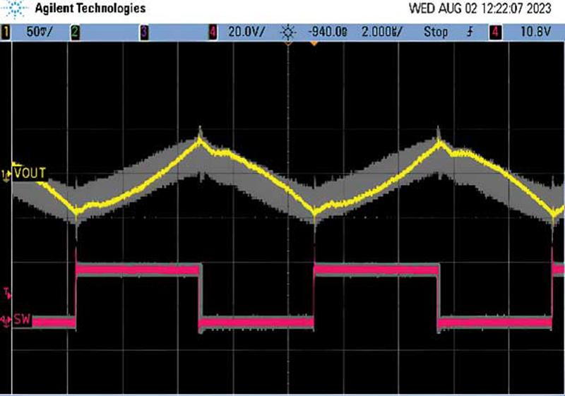
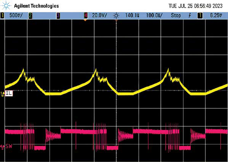
In addition, with higher valued inductors, the saturation current rating is usually smaller. This can lead to inductor saturation, which is dangerous for the deviceas discussed in the Saturating the Inductor section. The effect of saturating an extremely oversized inductor can be seen in Figure 8.
Click image to enlarge
Figure 8. Saturated inductor output waveform with inductor that is 22 times the nominal value. The current rating does not increase proportionally with inductance
To mitigate this issue, the output voltage ripple can be controlled by altering the output capacitors that were chosen. By either increasing the value of the output capacitor or decreasing its ESR, the output voltage ripple can be reduced without having to increase the inductor’s value. This will allow the inductor current ripple to stay at a value between 30% and 40%, allowing the sensing architecture to properly acquire the signal.


