Part 3 of a 6 part series: Application Trends in SiC
SiC Applications in Electric Vehicle (EV) Power Conversion
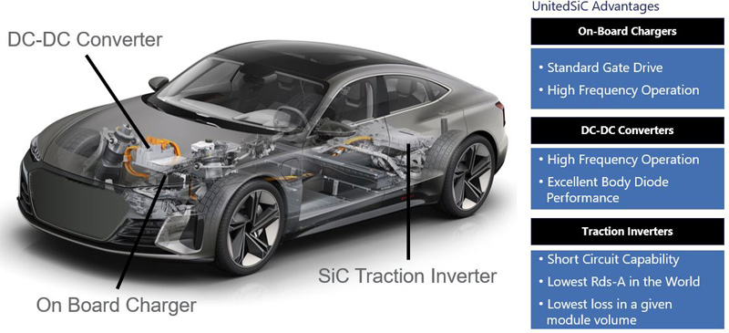
Electric vehicles (EVs) are seeing rapid growth in shipments, with a great deal of acceleration expected in the 2020s. All major car manufacturers have introduced or have firm plans for EV models and are actively engaged with their partners in researching the best power electronics to maximize range and minimize costs. The main applications for SiC devices are shown in Figure 1, and forecasts show the potential for $10B in SiC shipments by 2030. The highest power element is the EV Traction inverter, which we discuss in a future article. The other main converters are the on-board charger and DC-DC converter. They increasingly involve bi-directional power flow and benefit greatly from fast switches with excellent body diode behavior. SiC FET offerings are now available with AEC-Q101 qualification to meet these needs. We discuss the main topologies, and examine the advantages of using SiC devices, especially in the higher battery voltage systems (500-800V).
Click image to enlarge
Figure 1: UnitedSiC Advantages
On-Board charger topologies
Since the on-board charger (OBC) is located within the car, it is necessary to save volume and weight by using a converter topology that maximizes both power density and efficiency. The choice of topology can depend on the power range, which can be 6.6KW, 11KW or even 22KW in passenger EVs. In some cases, the OBC may be bidirectional, which means that not only does the circuit allow the battery to be charged from the grid, your EV can serve as a distributed energy source that feeds energy back to the grid. In that mode, power flow is reversed but the peak operating power may be lower (half) of the battery charging rate.
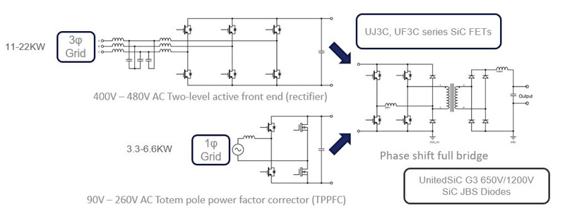
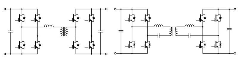
Figure 2shows two configurations found in on-board chargers designed for unidirectional power flow. The circuit has two main sections, a frontend rectifier stage, and a DC-DC converter stage. The rectifier stage rectifies the AC mains voltage to provide a DC rail with unity power factor. The DC-DC phase-shifted-full-bridge stage then provides accurately controlled output to charge the battery pack. During Li-ion battery charging, the circuit operates first in a controlled current mode, then a constant power mode for rapid charging, and finally a constant voltage mode until the battery is charged.
Click image to enlarge
Figure 2: Two configurations found in on-board chargers designed for unidirectional power flow
To maximize efficiency in the rectifier stage, bridgeless topologies are increasingly popular, since the conduction losses of the diode rectifier bridge can be avoided. Figure 2 shows the Totem-Pole PFC (TPPFC) circuit that can be used for lower power levels. This circuit involves a fast switching phase leg while the other switches at line frequency. The fast switching leg may be operated in continuous conduction mode (CCM) or Critical Conduction Mode (CRM). In CCM mode, the switch turn-on is hard, and the best option is to use wide bandgap switches with their excellent low QRR body diodes. Figure 3 shows a comparison of the device parameters, including QRR of UnitedSiC FETs compared to state of the art Superjunction devices. For switching frequencies above 20kHz, it is necessary to use wide-bandgap switches, and the standard gate drive offered by UnitedSiC FETs makes the drop-in & upgrade transition from Superjunction device-to-UnitedSiC FET easier.

Click image to enlarge
Figure 3: Comparison of the device parameters, including QRR of UnitedSiC FETs compared to state of the art Superjunction devices
If the CRM mode is used, then the peak currents become higher, putting additional constraints on the inductors, and requiring lower on-resistance switches. The absence of hard turn-on allows the use of Silicon Superjuncton FETs, at least at lower bus voltages. Even in this situation, using SiC FETs makes sense due to the very low on-resistance options now available, and increasing competitive pricing relative to Superjunction FETs with similar on-resistance. Furthermore, the topology can be extended to higher DC rail voltages with 1200V SiC FETs, to increase power output with minimal switch count.
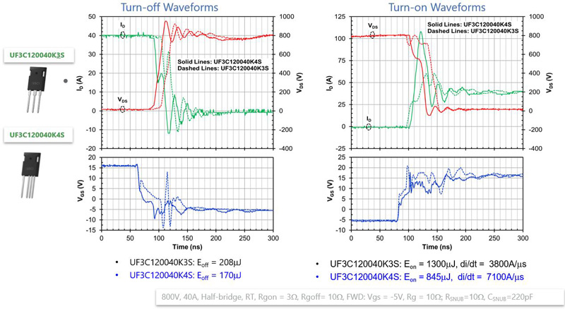
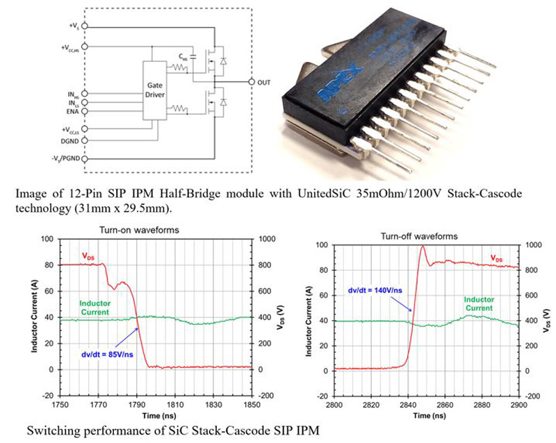
The 3-phase active frontend rectifier is an excellent option for higher power levels 11-22KW. The bus voltage is typically 600-800V, which requires the use of 1200V devices. Again, the two-level 3-phase circuit of figure 2 requires switches with low switching losses and low QRR, which shifts the choice towards SiC FETs instead of IGBTs. Figure 4 shows the turn-on and turn-off characteristics of the 35mohm, 1200V, TO247-4L (UF3C120040K4S) UnitedSiC FAST FET. These devices are used in parallel to implement the active frontend rectifier with high efficiency, given their very low turn-on and turn-off losses. Using the 4-leaded Kelvin package, users can switch faster with lower losses and cleaner gate waveforms.
Click image to enlarge
Figure 4: Turn-on and turn-off characteristics of the 35mohm, 1200V, TO247-4L (UF3C120040K4S) UnitedSiC FAST FET
An alternate approach to the frontend rectifier is the Vienna rectifier, shown in figure 5, which allows the use of 650V Silicon Superjunction devices along with SiC Schottky diodes to reduce cost. In this circuit, the switches do not undergo hard switching. The number of semiconductors required is higher, and diode drops limit the best achievable efficiency.

Click image to enlarge
Figure 5: Vienna rectifier, which allows the use of 650V Silicon Superjunction devices along with SiC Schottky diodes to reduce cost
DC-DC converters
As shown in figure 2, the workhorse DC-DC converter for both battery charging and supplying 12V/24V power is the phase shift full bridge. At full load, this circuit operates with zero-voltage-switched (ZVS) turn-on of the FETs, and turn-off loss is minimized with a snubber capacitor across the device. The circuit can be operated at high frequencies (100-300kHz) with good efficiency. The low conduction and turn-off losses of SiC FETs make them ideal, especially since their gate drive requirements are also simple. This is the case with UnitedSiC FETs that can be driven with 0 to 12V, or from a simple pulse transformer that outputs -12/0/12V. In light load conditions, hard switching might occur, which makes the Superjunction FETs problematic and more prone to diode recovery induced failure, and IGBT circuits prone to elevated losses.
The LLC topology shown in figure 6 is an excellent choice, especially when the output voltage is fixed. This topology is found most often in the fixed output DC-DC converter stage, while the phase-shift full-bridge is considered more suitable for dealing with variable output voltage. At lower bus voltages, Superjunction FETs with fast diodes are used in LLC circuits. At higher voltages, IGBT losses become excessive and the choice shifts to SiC FETs.
Click image to enlarge
Figure 6: At lower bus voltages, Superjunction FETs with fast diodes are used in LLC circuits. At higher voltages, IGBT losses become excessive and the choice shifts to SiC FETs
Even at lower bus voltages, UnitedSiC 650V SiC FETs offer very low gate charge, low time to charge the output capacitance and low body diode conduction loss, that can be used to drive up LLC operating frequencies from 100kHz to 500kHz. On-resistances as low as 7mohm 650V are now available in the TO247-4L package. For low profile space constrained applications, a 27mohm, 650V device is available in the industry standard DFN8x8.
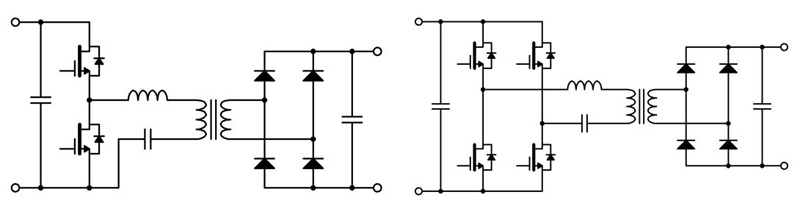
For bi-directional DC-DC conversion, figure 7 shows the dual active bridge (DAB) and CLLC circuits, where the output side has active switches. For battery charging, since the output voltage varies widely, the DAB can be controlled from a fixed DC bus by varying the gate PWM waveforms. If the CLLC topology is applied, then to maintain operation near resonance for the DC-DC stage, the bus voltage must be varied by changing the control scheme on the active rectifier stage (Totem pole PFC or 3-phase active frontend). In either case, it becomes necessary to use SiC FETs on the secondary side to efficiently hard-switch in the inversion mode. These may be 650V to 1200V FETs for EV battery charging, or lower voltage silicon FETs in the 100-150V class for 12V/24V outputs.
Click image to enlarge
Figure 7: Dual active bridge (DAB) and CLLC circuits, where the output side has active switches
Easing the transition
Wide bandgap SiC FETs enable the use of improved topologies and higher frequencies to achieve the targets of high-power density and efficiency. The higher cost of the switches is easily offset by the system level gains in the EV space. UnitedSiC FETs provide a key benefit of being compatible with all types of gate drive voltages, so they can be dropped into silicon-based designs, as well as SiC MOSFET designs. This eases the transition for designers around the world as they increasingly deploy SiC, sometimes just to upgrade existing silicon-based designs.
What’s on the horizon
The next stage is likely to involve integrated driver and FET stages, such as the SIP half-bridge with driver shown in figure 8, using 35mohm, 1200V stack cascode switches. The switching waveforms show the very fast and clean switching enabled by such a device, which can be used as a building block for all the circuit options described in this article.
Click image to enlarge
Figure 8: Integrated driver and FET stages, such as the SIP half-bridge with driver shown, using 35mohm, 1200V stack cascode switches
SiC FET technology improves rapidly, with 2X improvements in switching figures of merits under development for 2020 release. Coupled with discrete package improvements and the introduction of SiC based intelligent power modules, these advances will help push power density further as EV deployment continues to ratchet up.
UnitedSiC