Balancing Speed and Stability in Parallel-Connected SiC MOSFETs Designs

In high-power systems, small instabilities can cause major performance issues
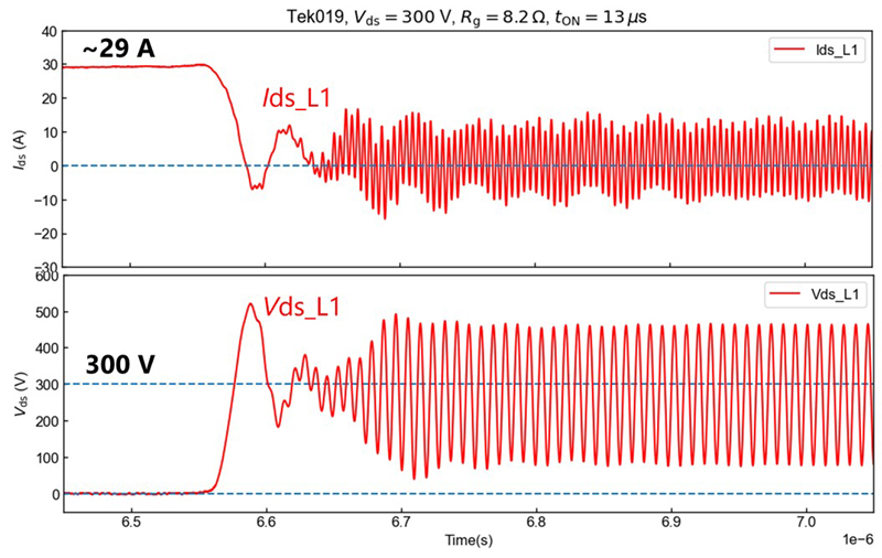
Figure 1: Stability versus Current
- Low current condition (Vds=200V)
- High current condition (Vds=200V)
Engineers working with Silicon Carbide (SiC) MOSFETs encounter this firsthand when parallel devices begin exhibiting unexpected oscillations. What starts as a subtle waveform irregularity on an oscilloscope trace can quickly reveal deeper design sensitivities in high-speed switching environments.
Parallel-connected SiC MOSFETs are increasingly employed in high-power applications, including electric vehicles, renewable energy systems, and industrial motor drives. Although parallel configurations facilitate substantial current loads, they present challenges related to stability, particularly oscillatory behavior.
Research Focus: Stability Optimization
This article provides an overview of strategies for mitigating oscillation phenomena in parallel-connected SiC MOSFETs. Variations in device parameters, such as threshold voltage (Vth) or on-resistance (Ron), as well as disparities in parasitic inductances, can induce oscillations.
To address these challenges, suppression techniques were examined by evaluating switching characteristics under a range of voltages, currents, and gate resistances in parallel configurations. Additionally, a simulation model was developed to accurately predict oscillatory behaviors. This article analyzes design parameters effective in minimizing oscillations and discusses the associated trade-offs with system performance.
Oscillation Challenges in High-Speed SiC MOSFET Switching
High-speed operation is vital for SiC MOSFETs to minimize switching losses. Even minor timing differences between parallel devices can produce unexpected oscillations, transforming a stable circuit into a testing challenge. Increasing gate resistance can suppress these oscillations. It also leads to higher losses, underscoring the importance of pinpointing the precise conditions that trigger instability and adjusting parameters accordingly.
In parallel SiC MOSFET circuits, oscillations were measured during switching across various voltages, currents, and gate resistances, while the effects of inductance imbalance and device characteristic variations were also assessed. These measurements revealed how small mismatches could result in noticeable instability.
This approach examined oscillation by systematically varying voltage, current, and gate resistance during switching. Although higher gate resistance reduces oscillations, it increases switching losses, requiring careful optimization. This study found that mismatches in stray inductance and device parameters - such as threshold voltage and on-resistance - can result in uneven current sharing and localized oscillations, particularly during high-speed switching. The results emphasized the critical role of selecting suitable gate resistance, minimizing layout-induced stray inductance, and matching device characteristics to suppress oscillations while enhancing reliability in high-power applications.
Key Findings: How Electrical and Device Parameters Shape Oscillation Behavior
By observing how current, voltage, device mismatches, gate resistance, and transconductance (gm) influence behavior, a complete picture emerges of the mechanisms that drive instability in parallel SiC MOSFETs.
Current dependence on oscillation
The circuit’s stability decreased as the current increased (see Figure 1). At low currents, parallel-connected SiC MOSFETs showed minimal oscillations with smooth switching. As current rose, oscillations intensified due to amplified effects from parasitic inductances and device mismatches, causing uneven current sharing and localized voltage spikes. Beyond a certain threshold, these oscillations became frequent and severe, posing reliability risks. Monitoring current levels and optimizing layout and component choices are essential to minimizing instability. At low currents, the system remained stable with minor oscillations. At high currents, fluctuations became larger and more frequent, emphasizing the need for matching device parameters and reducing parasitic elements for reliable operation under heavy loads.
Voltage dependence on oscillation
Circuit stability declined as operating voltage increased (see Figure 2). At lower voltages, waveforms were smooth and stable, but higher voltages - especially during switching - caused noticeable fluctuations and transient spikes. Oscillations grew more pronounced as voltage surpassed critical thresholds.
Instability manifested as transient voltage peaks and uneven current sharing among the parallel SiC MOSFETs, amplifying the effects of parasitic elements. Low-voltage conditions yielded minor oscillations, while higher voltages led to greater magnitude and frequency of oscillations, demonstrating a strong link between load voltage and instability.
This escalation distorts waveforms and raises concerns about device stress and long-term reliability. These results emphasize the need for design optimization, such as adjusting gate parameters and layout, to effectively manage oscillations and ensure stability in high voltage power systems.
Click image to enlarge
Figure 2: Stability versus Voltage
- High voltage condition (Vds=300V)
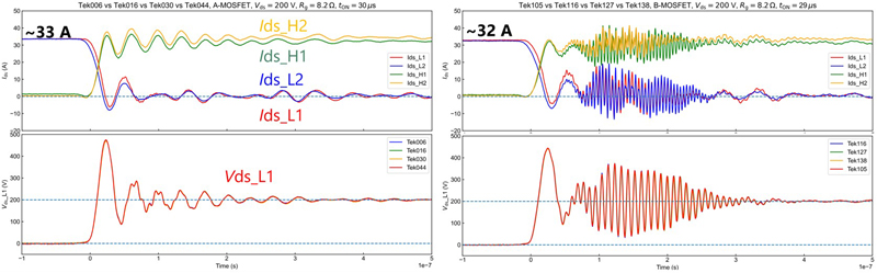
Device parameter dependence
The evaluation of parallel SiC MOSFET circuits shows that variations in key device parameters - including threshold voltage (Vth) and on-resistance (Ron) - significantly affect oscillation. Closely matched devices enable even current sharing and stable switching. In contrast, increased differences in Vth and Ron result in uneven current sharing, causing more frequent and severe voltage and current spikes, particularly at higher currents where parasitic effects intensify. These findings underline the importance of selecting devices with similar characteristics, carefully designing to minimize parameter variations, suppressing oscillations and ensuring reliable high-power SiC MOSFET operation (See Figure 3).
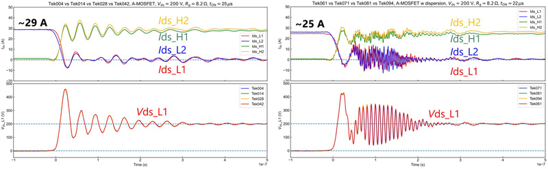
Click image to enlarge
Figure 3: Oscillation versus Device variation
- Small variation in device characteristics
- Larger variation in device characteristics
External gate resistance dependence
Gate resistance (Rgex) influences oscillations, shown in Figure 4. With an external Rgex of 8.2Ω, oscillations occurred; reducing Rgex to 2.7Ω suppressed these oscillations but increased ringing. This result demonstrates a trade-off between two design objectives:
· Oscillation suppression: Lowering the shared resistor (Rgex) among parallel MOSFETs attenuates the signal in Loop1 (Figure 5), diverting some to ground suppressing oscillation. If Rgex is too high, attenuation is insufficient, making oscillations more likely.
· Ringing minimization: A larger Rgex can suppress oscillation in Loop 2, helping to minimize ringing.
Optimizing external gate resistance is crucial for balancing switching stability and signal integrity. The chosen Rgex must consider both oscillation suppression and ringing minimization, based on application and layout conditions.
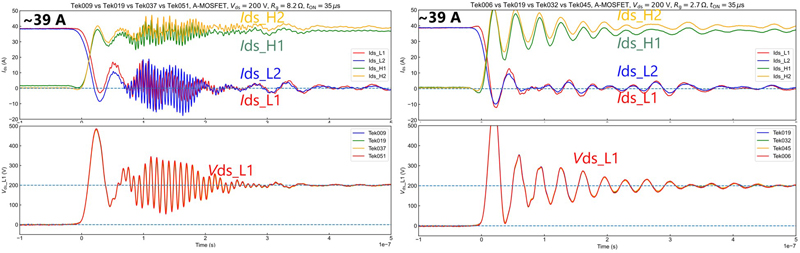
Click image to enlarge
Figure 4: Impact of Gate Resistance
- Large gate resistance (Rg=8.2Ω)
- Small gate resistance (Rg=2.7Ω)
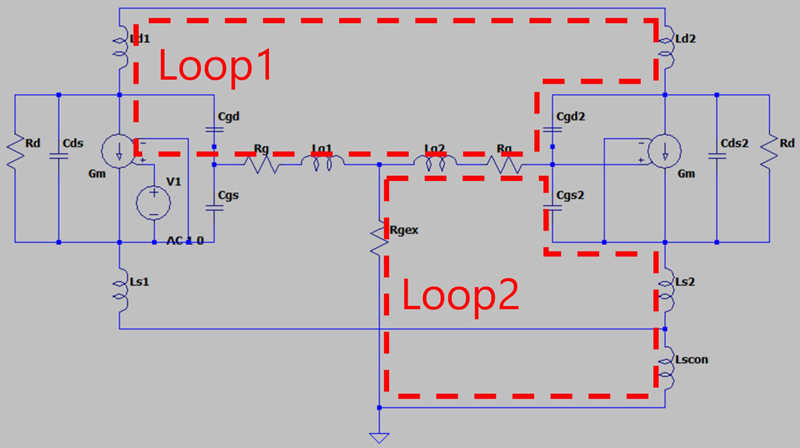
Click image to enlarge
Figure 5: Current Loops
- Diagram of oscillation in parallel-connected MOSFETs
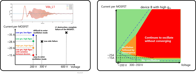
Impact of Large gm
Large gm readily induces oscillation, even at lower currents. Circuits with higher gm show pronounced oscillatory behavior. Increased gm heightens sensitivity to parasitic effects and device mismatches, making oscillations more likely, including sharper waveform transitions and ringing, as shown in Figure 6. In contrast, circuits with small gm display smoother switching, minimal oscillations and lower transient amplitudes. Lowering gm dampens parasitic impacts and device mismatches, resulting in more reliable operation and less device stress. Overall, gm plays a critical role in oscillatory tendencies, emphasizing the need for careful optimization in parallel SiC MOSFET applications.
Small gm yields gradual switching transitions and suppresses oscillations, supporting stability. Larger gm causes rapid transitions and intensifies oscillatory behavior - even at lower currents.
Click image to enlarge
Figure 6: Impact of gm on ringing
- Small gm.
- Larger gm.
Simulation analysis
Oscillation behavior in parallel-connected SiC MOSFETs was examined through SPICE simulations and experimental measurements. The results closely matched experimental data, validating the accuracy of the modeling for high-performance power systems.
To investigate conditions that trigger oscillation, key parameters such as gm and Rgex were varied. The findings summarized in Figure 7, reveal:
- Experimental results: Low gm and low Rgex combinations effectively suppress oscillations, while high gm and high Rgex combinations promote strong oscillations, particularly when device variations are present.
- Simulation classification: SPICE analysis categorizes behavior into three regions - stable (green), temporarily unstable (yellow), and continuously unstable (red).
This classification defines clear boundaries between stable and unstable operation. The strong alignment between simulation and experimental results demonstrates the effectiveness of SPICE modeling in predicting and mitigating oscillation issues in parallel-connected SiC MOSFET systems.
Click image to enlarge
Figure 7: Measurement versus Simulation
- Oscillation observation in experiment
- Oscillation parameters clarified by simulation
Recommendations: Design Guidelines for Reducing Oscillation
From these findings, several practical strategies can help minimize oscillations while maintaining high-speed performance in parallel SiC MOSFETs:
· Optimize gm: Lowering gm can help reduce oscillation sensitivity.
· Adjust Rgex carefully: While decreasing Rgex can suppress oscillations, it may increase ringing, making a balanced approach necessary.
· Ensure parameter matching: Aligning characteristics between devices, including Vth and Ron, is essential for minimizing instability.
· Consider high voltage and current effects: As higher voltage and current intensify oscillations, considering circuit design is crucial.
Practical Application: Implementation in Commercial SiC Power Modules
Toshiba has used these and other techniques to advance parallel SiC device technology that improves power modules, reduces parasitic oscillation and boosts energy efficiency. Real world examples include:
· Parasitic Oscillation Mitigation: Optimized Lg/Ls ratio to lower gate resistance in SiC modules, enabling high-speed switching and reduced power loss for renewable energy, railways, and industrial converters.
· High-Power Module Optimization: Addressed mutual and stray inductance and thermal fatigue in 3.3-kV/800-A SiC modules - critical for high-voltage industrial applications.
· Resin-Insulated Modules: Used distributed chip layouts and AI-based design to increase power density and reduce thermal resistance by 21%, enabling further miniaturization for renewables, railways, and automation.
Overall Insights and Engineering Takeaways
Through experimental measurements and simulation modeling, strategies to mitigate oscillations and solutions were proposed to optimize SiC MOSFET-based power systems for use in parallel-connected applications. These include adjusting gate resistance values, reducing stray inductance, and ensuring consistency in device characteristics. The results provide guidance for engineers seeking to improve the performance and reliability of high-power SiC MOSFET applications while addressing issues related to oscillation.


